Configurable, Analog-Focused MCUs for Sensor Interfacing Designs
The PIC18-Q71 MCUs product family combines powerful Core Independent Peripherals (CIPs) and a high level of analog integration to simplify sensor interfacing and analog measurements, optimize system performance and reduce BOM cost. PIC18-Q71 MCUs contain a 12-bit differential Analog-to-Digital Converter (ADC), configurable Operational Amplifiers (OPAs), high-speed analog comparators and an 8-bit signal routing port to interconnect digital peripherals. These MCUs have extended timing capabilities for precision control with integrated high resolution 16-bit dual Pulse Width Modulators (PWMs), a 20-bit Numerically Controller Oscillator (NCO) and a 32-bit Universal Timer (UT). Their rich set of CIPs, in combination with the Analog Peripheral Manager (APM), enable simple analog configurations and quick responses to system events. You can easily configure peripherals and functions, generate application code and simulate analog circuits prior to hardware prototyping to reduce your development time and speed up your time to market. This product family is available in package and memory options for a variety of applications including LED lighting, predictive maintenance, medical, home automation, industrial process control, automotive and Internet of Things (IoT).
Try Live PIC18-Q71 Demos
Are you an embedded application engineer starting your next design and looking to take advantage of the on-chip Core Independent Peripherals (CIPs)? Do you find yourself looking for a hands-on experience to understand how these features work in real time? Now, you can interact with physical demos on your screen from anywhere. Microchip Try is a website for visual learners that provides real-time demos that you can interact with by changing variables and watching how the demo responds.
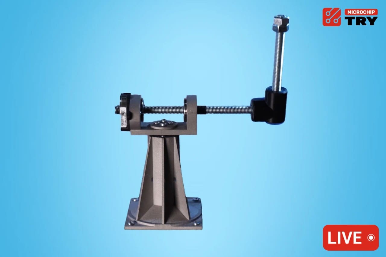
Explore the real time control demo and the Operational Amplifier (OPA) cloud lab demo, engage with it, and learn how to implement the features in your design.

Getting Started
The PIC18F56Q71 Curiosity Nano Evaluation Kit is the best platform for rapid prototyping with the PIC18-Q71 family of MCUs. This USB-powered kit features an on-board programmer/debugger that seamlessly integrates with MPLAB® X Integrated Development Environment (IDE). Its small form factor makes the board excellent for breadboard soldering, or you can combine it with the Curiosity Nano Base for Click boards™, which features multiple mikroBUS™ sockets so you can easily add sensors, actuators or communications interfaces from Mikroelektronika’s extensive selection of Click boards.

System Features
Configurable Analog
12-bit ADCC, OPAs, 8/10-bit DAC and ZCD
The intelligent ADC, configurable OPAs, high-speed analog comparators, multiple Digital-to-Analog Converters (DACs) and a Zero Cross Detect (ZCD) peripheral offer a high level of analog integration for amplification, filtering and signal conditioning for sensing and measurement applications. With the 12-bit differential ADC with Computation (ADCC) and context switching, you can achieve high-resolution ADC conversions with strong noise rejection, automated analog signal analysis and data acquisition functions for enhanced real-time system response. The programmable gain settings of the on-chip OPAs reduce the cost and space required by external components in applications that require a gain stage before ADC conversions.
Layout Flexibility
Peripheral Pin Select (PPS)
PPS provides ultimate flexibility when routing digital signals to device pins. With PPS, you can connect any digital peripheral to any I/O pin on the fly for a customized layout. This allows you to maintain layout compatibility with older PIC® MCUs, even as new features are implemented.
Hardware Customization
Custom Logic and Interconnections
You can easily customize the configurable peripherals to fit your application needs. The 8-bit signal routing port interconnects digital peripherals without external pins, which enables rapid response to changing events in commonly used control systems. The Configurable Logic Cell (CLC) is a user-configurable peripheral for creating custom, hardware-based logic functions. The CLC peripheral lets you integrate a combination of external and internal signals as inputs and connect on-board peripherals to reduce the number of external components needed for your design, which reduces your PCB footprint and overall system cost.
Power-Conserving Functionality
IDLE, DOZE, Peripheral Module Disable (PMD)
IDLE and DOZE low-power modes optimize your application for device performance and power consumption. PMD turns off unused peripherals individually, further reducing power consumption.
Design Flexibility
Configurable Timers and 16-bit PWM
You can combine the two customizable 16-bit UTs to make a larger timer to deliver advanced capabilities beyond those found on standard timer modules. The integrated, high-resolution 16-bit PWMs allow you to easily vary phase and duty cycle and offset event count with greater precision, providing advanced capabilities beyond those found on standard PWM modules. The flexible serial communications interface options include a UART with support for asynchronous, DMX and LIN protocols, plus higher-speed, standalone I2C and SPI modules.
Safety First
Functional Safety Ready
The CRC/SCAN module and the Windowed Watchdog Timer (WWDT) work in tandem to provide the necessary tools to incorporate functional safety into your application. By ensuring the integrity of the program Flash contents, the devices support the implementation of safety standards such as Class B and UL 1998.
Improved System Response
CIPs
The configurable CIPs require almost no additional code and no additional components to enable this family of MCUs to handle and accomplish mission-critical and time-sensitive tasks smoothly and entirely without CPU intervention. They save Flash memory and allow you to use the CPU’s resources to run complex systems as efficiently as possible. This combination of benefits simplifies your design while reducing power consumption and increasing system responsiveness.
Improved System Performance
Direct Memory Access (DMA)
The PIC18 Q71 family features four DMA controllers that quickly transfer data between different memory locations without any CPU interaction. You can use DMA techniques, such as configuration context switching, to reduce power consumption while increasing your system’s performance.