Versatile Microcontrollers family with Multi-Voltage I/O and Programming and Debugging Interface Disable
The PIC18-Q24 MCUs series enhances flexibility and security for high-pin-count PIC18 MCUs. This family of MCUs introduces the Programming and Debugging Interface Disable (PDID) feature, which disables the ICSP interface to prevent any external access or modifications to memory. It also supports applications that require an immutable secure bootloader. The PIC18-Q24 family is the first series of PIC® MCUs to offer Multi-Voltage I/O (MVIO), which enables true level-shifted, bi-directional communication with devices on a different voltage domain with up to twelve pins on the additional voltage domain. These 28-, 40- and 48-pin devices are equipped with a 10-bit Analog-to-Digital Converter with Computation (ADCC) with a sampling rate of up to 300 ksps, two dedicated SPI and I2C modules, four Direct Memory Access (DMA) channels, six 16-bit Pulse-Width Modulation (PWM) outputs, two Universal Timers (UTs) and two Zero Cross Detect (ZCD) modules. The combination of these features makes the PIC18-Q24 family an excellent choice for IoT, industrial automation, automotive, consumer electronics and energy management applications.
Getting Started
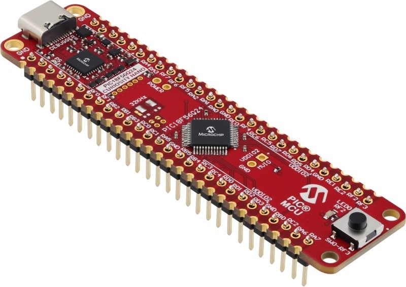
Take your next idea to market with a development board that you can keep in your pocket. With full program and debug capabilities, the PIC18F56Q24 Curiosity Nano Evaluation Kit offers complete support for your next design.
The PIC18-Q24 family is designed to integrate with MPLAB® Code Configurator (MCC), a free software plug-in for our award-winning MPLAB X Integrated Development Environment (IDE) that provides a graphical interface to configure peripherals easily and functions specific to your application. To simplify development over multiple voltage domains, MCC has MVIO drivers that will help you set up this peripheral quickly. Code examples are also available to help you immediately start your development.

System Features
Programming and Debugging Interface Disable
PDID
This function disables the connections to the device’s memory by locking the memory and preventing it from being accessed through the standard programming and debugging interface.
Support for Multiple Voltage Domains
MVIO
The Multi-Voltage IO (MVIO) feature allows the MCU to interface with digital inputs or outputs at a different operating voltage than the rest of the device. The MVIO feature reduces system costs, design complexity and board space by replacing external level shifters with internal level shifters.
Configurable Analog
10-bit ADCC
The high-speed ADCC automates signal analysis and data acquisition functions, which simplifies the development of real-time control and capacitive sensing designs.
Design Flexibility
Configurable Timers, 16-bit PWM
The two customizable 16-bit Universal Timers (UTMRs) can be combined to make a larger timer that delivers advanced capabilities beyond those found on standard timer modules. The integrated, high-resolution 16-bit PWMs provide advanced capabilities beyond those found on standard PWM modules. They allow you to vary phase, duty cycle and offset event count easily and with greater precision.