Intelligent, Fast and Accurate Analog series of tinyAVR® MCUs
The ATtiny1627 family of AVR® microcontrollers (MCUs) is equipped with high-speed integrated analog, hardware-based Core Independent Peripherals (CIPs) and low-power performance for efficient real-time control and sensor node applications. For design flexibility and to optimize your board layout, this family of 4 KB to 32 KB Flash devices is available in SOIC, SSOP and VQFN packages ranging from 14 to 24 pins. These tinyAVR® MCUs are well suited for a wide range of industrial, consumer, appliance, automotive, sensor node and other applications. If your design is a closed-loop control system, the ATtiny1607 family is a great option.

Enabling Reliable Sensor Interfaces in Harsh Environments
Take Your Idea from Concept to Prototype
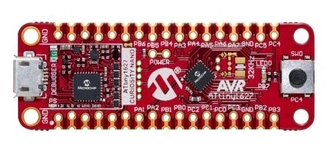
The ATtiny1627 Curiosity Nano board is the ideal platform for rapid prototyping with these tinyAVR MCUs. This USB-powered kit features an on-board programmer/debugger that seamlessly integrates with the MPLAB® X Integrated Development Environments (IDE). Its small form factor makes it excellent for breadboard soldering, or you can combine it with the Curiosity Nano Base for Click boards™, which features multiple mikroBUS™ sockets so you can easily add sensors, actuators or communications interfaces from Mikroelektronika’s extensive selection of Click boards.
- MPLAB X IDE Projects
- Training Videos (Six episodes on getting started with the 12-bit differential ADC and PGA)

Functional Safety Ready for Safety-Critical Applications
Our ATtiny3227 family for safety-critical applications targets both industrial and automotive products. We also offer the MPLAB XC8 Functional Safety Compiler License, which is a TÜV SÜD-certified compiler package that supports 8-bit PIC® and AVR MCUs. Our ATtiny3227 ISO 26262 and IEC 61508 functional safety packages come with documents such as FMEDA reports and safety manuals.
System Features
Real Time Response
Event System
The Event System allows peripherals to communicate directly with each other without involving the Central Processing Unit (CPU) or bus resources. The Event System network is independent of the traditional data bus paths. This means that different triggers at the peripheral level can result in an event, such as a timer’s interrupts triggering an action in another peripheral. The Event System has three independent channels for direct peripheral-to-peripheral signaling. This is a deterministic signaling method and a perfect fit for real-time applications. The events are handled at the peripheral level whether the CPU is occupied handling interrupts or in sleep mode.
Safety First
CRC, WWDT, BOD, POR, VLM
You can use the built-in features that support safety-critical applications to add robustness and reliability to your design. These include the Windowed Watchdog Timer (WWDT) for system supervision, the Cyclic Redundancy Check (CRC) for scanning Flash memory, and the Event System for fault detection. Other features include a Voltage Level Monitor (VLM), a Brown-Out Detector (BOD) and Power-On Reset (POR) for monitoring the supply voltage.
Hardware Customization
Custom Logic
The Custom Logic peripheral is a programmable logic peripheral that can be connected to the device pins, events or other internal peripherals. Each Lookup Table (LUT) consists of three inputs: a truth table, an optional synchronizer and a filter and edge detector. An LUT can generate an output to be routed internally or to an I/O pin. This eliminates the need for external logic and reduces BOM cost.
Integrated Analog
12-bit ADC, PGA, Analog Comparator
The on-chip 12-bit, 375 ksps differential Analog-to-Digital Converter (ADC) features selectable internal voltage references with minimal temperature drift. Use the hardware averaging and oversampling to improve noise suppression and accuracy for analog inputs. Averaging and threshold detection enable the MCU to remain asleep for longer periods, significantly reducing power consumption.
The Programmable Gain Amplifier (PGA) supports up to 16x gain making it possible to retrieve small signals in noisy environments.
Power-Conserving Functionality
Idle, Standby, Power-Down
Idle and Standby low-power modes allow you to optimize your application for device performance and power consumption. The Power-Down allows unused peripherals to be turned off individually, further reducing power consumption.