A disruptive technology over the century-old quartz oscillator, Microelectromechanical Systems (MEMS)-based oscillators have received wide market adoption in recent years due to the reliability, short lead times and small package sizes. As the leader in this rapidly growing market, we can help you identify solutions for your timing needs. We offer industry’s most complete MEMS-based timing solutions that include both single output oscillators that are drop-in replacements to the traditional quartz oscillators and multiple output clock generators that can provide a highly reliable and accurate reference clock to your system without the need of an external reference crystal.
Silicon MEMS-based timing devices offer high reliability (including AEC-Q100 certification for automotive use), wide operating temperatures (−55⁰C to 125⁰C), superb shock and vibration resistance, high accuracy (±10 ppm) and small size (1.6 mm × 1.2 mm).
MEMS oscillators provide a reliable, efficient, cost-effective solution for precise timing and synchronization needs across diverse industries. We offer several compelling advantages for your design.
- Precision and Stability: Exceptional timekeeping and synchronization across various applications
- Size and Integration: Extremely small and compact timing devices for space-constrained applications
- Durability and Reliability: Resistant to shock, vibration and temperature variations, which makes them reliable in harsh environments
- Low Power Consumption: Consume less power than traditional quartz-based timing devices, which is crucial for battery-operated and portable devices
- Shorter Time to Market: Streamline your development process with our flexible configuration and quickly obtain the precise frequency you need
Featured Products
DSC612/613
Smallest Multi-Output MEMS Clock Generators
These MEMS clock generators provide a single-chip, multi-output solution for microcontroller (MCU)-based systems. These flexible solutions cover a wide frequency range without requiring an external crystal, which saves power and reduces board space by up to 80%.
DSC15xx
Ultra-Low-Power, Low-Jitter MEMS Oscillators
These low-jitter, ultra-low power and high-stability oscillators are available for a wide supply voltage range of 1.71V to 3.63V and temperature range of −40°C to +125°C. This MEMS-based design features a robust all-silicon resonator, offers high reliability and is great for rugged industrial and portable applications.
HTM61xx and M9xxxxx
Military-Grade MEMS Oscillators
These oscillators meet the MIL-STD-883 and MIL-STD-202 standards for temperature, shock, vibration and solderability. They can withstand extreme conditions, including 70g vibration and 50 kg shock. These oscillators are available in ultra-small packages with customizable frequency output and an optional tin-lead solder dip.
DSA12xx
High-Performance Automotive Oscillators
Our automotive-grade, high-performance oscillators feature advanced silicon MEMS technology for reduced close-in noise. These oscillators provide exceptional jitter and stability across various voltages and temperatures. The 2.5 mm × 2.0 mm package option is the smallest differential oscillator on the market.
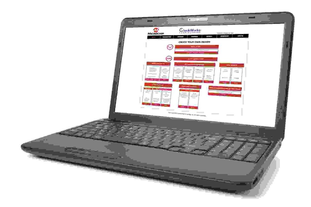
Clockworks® Configurator
Customize and Order Samples
With just a few clicks, configure your MEMS-based oscillators and get fast samples with this easy-to-use online tool.
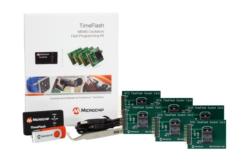
TimeFlash Field Programming Kit
Any Frequency, Anywhere
Easily program your MEMS-based oscillators to a custom frequency in seconds using this field programming kit.
- Application Notes
- Brochures
- Other
- White Papers
- FAQs
|
Title
|
|
|---|---|
| Measuring Spread Spectrum Modulation | Download |
| PCIE Signal Integrity and EMI | Download |
| Quartz Crystals and Micrel ICs | Download |
| Microchip MEMS Oscillator and Clock Products for Automotive Applications | Download |
| Differential Clock Translation | Download |
| Jitter Blocker | Download |
| MEMS Oscillators Offer Immunity to EMI | Download |
| PECL Waveform Measurements | Download |
| Immunity of MEMS Oscillators to Mechanical Stresses | Download |
| Alignment of Non-50 Percent Duty Cycle Output Clocks | Download |
| Schematic Review Checklist for Microchip Timing Devices | Download |
| Pre-Configured Clock Generator Part Numbers for Switchtec and Data Center Applications | Download |
| AN4287 - Oscillator Groups and Classifications | Download |
|
Title
|
|
|---|---|
| Oscillators - MEMS and Crystal Solutions Brochure | Download |
|
Title
|
|
|---|---|
| MEMS Clocks FAQs | Download |
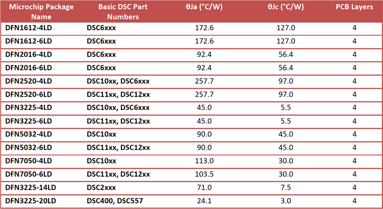
What are the Junction to Ambient (Theta JA) and Junction to Case (Theta JC) thermal resistance for the MEMS products?
Can a MEMS device select among different frequencies for a given output clock?
Is it possible to change the programmed output frequency?
What is the logic level for the input frequency select pins?
Are there MEMS devices that can generate two clock outputs from the same device?
How does the phase noise change with the carrier frequency?
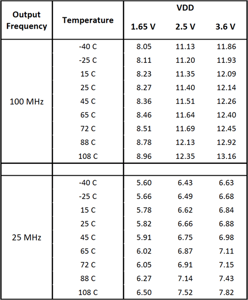
Does the supply current increase with the voltage supply and the clock frequency?
In addition to bypass capacitors, do you recommend using ferrite beads on the power supply (VDD)?
Can the MEMS devices latch up?
What is the difference between start-up time and enable time and how are they measured?
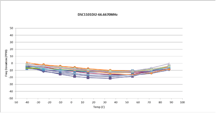
What is the frequency stability behavior over the temperature range?
Can the soldering process affect the frequency stability?
Can the MEMS oscillators/clocks work in a high-pressure environment, in particular up to 700 psi and surviving at 1,700 psi?
Video #1 - PCIe Overview
This 5-minute video provides the viewer with the fundamental concepts related to PCIe; it is the first video in a series that focuses primarily on the clocks and timing issues related to PCIe, and it also provides a basic understanding with which to explore further PCIe topics.
Intended Audience:
Anyone interested in an easy-to-understand high-level introduction to PCIe. No prior knowledge of PCIe is assumed.
What topics are covered?
1. Point-to-Point bus
2. Bi-directional bus
3. Scalability of data rates
4. Backwards compatibility
5. Wide adoption across many markets

TimeFlash MEMS Oscillators Field Programming Kit
TimeFlash MEMS Oscillators Field Programming Kit
This video provides a quick demonstration of the TimeFlash MEMS Oscillators Field Programming Kit that allows you to instantly program MEMS oscillators to any frequency, anywhere. This kit supports all Microchip MEMS oscillator package sizes and is designed to enable rapid prototyping and testing.

ClockWorks® Configurator Online Tool
ClockWorks® Configurator Online Tool
This video walks you through the features of the ClockWorks® Configurator online tool and shows you how to customize oscillators and clock generators. Find out how this easy-to-use tool also enables you to download data sheets order customized samples.
Need Help?

Request a Quote
Contact our Client Success Team to get more information about our clock and timing products or to request a quote.

Find Local Sales and Support
We have an extensive network of highly trained clock and timing experts. Go to our listing to locate a sales and support representative in your country.

Access Our Support Portal
Visit our Frequency and Time Systems support portal to download technical documents and other resources, enter support tickets or open RMA service requests.