Log in to myMicrochip to access tools and benefits. Sign up in just one minute.
Maximize Your Experience: Reap the Personalized Advantages by Completing Your Profile to Its Fullest! Update Here
Stay in the loop with the latest from Microchip! Update your profile while you are at it. Update Here
Complete your profile to access more resources.Update Here!

Part Number: INTRFCEV
PSRR AND DIGITAL NOISE EVALUATION BOARD
N/A
Overview
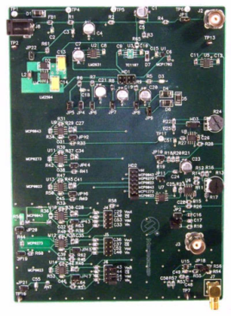
The PSRR and Digital Noise Evaluation Board supports measurement of Power Supply Rejection Ratio (PSRR) performance of Operational Amplifiers, as well as illustrates effects of Digital Interface spikes on Chip Select pins (and VDD, VOUT, VIN pins). The various measurements demonstrate importance of IDDQ on PSRR and Digital Noise performance.
A variety of Op Amps and Low Dropout regulators, and one Switching Regulator, plus selectable low-pass RC filters in VDD, allow the student to evaluate output (sinusoidal) noise versus sinusoidal frequency.
The PCB uses individual Gain=100 Op Amp circuits, plus Gain=10 output coaxial driver, achieving an referred-to-input resolution of 1 microvolt or less.
The PCB generates 0.25volt Digital Spikes, with 1nanoSec edges, for injection into an Op Amp. With DVM monitoring, sub-microvolt effects are easily observed.
An un-populated SMA footprint allows Radio Frequency injection, to examine Op Amp behavior with modulated BlueTooth or Cell Phone signals.
Package Contents
The PSRR and Digital Noise Evaluation Board (104-00139) is designed to explore and quantify the effects of power and digital noise on system performance. These experiments will help system designers understand the impact that power and digital noise can have in their design. The PSRR and Digital Noise Evaluation Board supports measurement of Power Supply Rejection Ratio (PSRR) performance of Operational Amplifiers, as well as illustrates effects of Digital Interface spikes on Chip Select pins (and VDD, VOUT, VIN pins). The various measurements demonstrate importance of IDDQ on PSRR and Digital Noise performance.
A variety of Op Amps and Low Dropout regulators, and one Switching Regulator, plus selectable low-pass RC filters in VDD, allow the student to evaluate output (sinusoidal) noise versus sinusoidal frequency.
The PCB uses individual Gain=100 Op Amp circuits, plus Gain=10 output coaxial driver, achieving an referred-to-input resolution of 1 microvolt or less.
The PCB generates 0.25volt Digital Spikes, with 1nanoSec edges, for injection into an Op Amp. With DVM monitoring, sub-microvolt effects are easily observed.
An un-populated SMA footprint allows Radio Frequency injection, to examine Op Amp behavior with modulated BlueTooth or Cell Phone signals.