
Silicon Carbide (SiC) MOSFET technology represents a major advancement in power electronics, helping you design more efficient, compact and reliable systems. SiC MOSFETs replace traditional silicon devices to enable lower switching and conduction losses with higher switching frequencies.
Choosing the Best Solution: The Advantages of Silicon Carbide MOSFETs Over IGBTs
Silicon Carbide (SiC) metal oxide semiconductor field (MOSFET) technology represents a major advancement in power electronics, helping you design more efficient, compact and reliable systems. SiC MOSFETs replace traditional silicon devices to enable lower switching and conduction losses with higher switching frequencies. These advantages help to reduce the component size and count and to reduce overall system size, weight and cost. SiC MOSFETs produce efficient, flexible and reliable high-voltage applications.
SiC MOSFETs are capable of higher temperature operation, faster switching and higher breakdown voltage, allowing for more efficient and more compact power electronics systems. SiC MOSFETs also have a much lower on-resistance, which results in lower power losses during operation. With added robustness and immunity to thermal runaway, SiC is better suited for high-power applications. Our mSiC™ MOSFETs cover 700V, 1200V, 1700V and 3300V (3.3 kV) SiC MOSFETs.
 |
In summary, SiC offers the following advantages over silicon:
- Higher operating temperature
- Higher breakdown voltage
- Lower on-resistance
- Faster switching speeds
- Improved ruggedness
Characteristics |
Results |
Benefits |
Breakdown field (MV/cm) |
Lower on-resistance |
Higher efficiency |
Electron saturation velocity (cm/s) |
Faster switching |
Size reduction |
Bandgap energy (EV) |
Higher junction temperature |
Improved cooling |
Thermal conductivity (W/m.K) |
Higher power density |
Higher current capabilities |
Positive temperature coefficient |
Self-regulation |
Easy paralleling |
Structure of mSiC MOSFETs
 |
In SiC MOSFETs, the source, drain and gate electrodes are separated by a SiC drift layer, which acts as the semiconductor. When a voltage is applied to the gate electrode, it creates an electric field that controls the flow of current between the source and drain electrodes.
Gate Oxide Stability
After 1000 hours of accelerated stress under both negative and positive gate bias, third-party testing shows virtually no change in threshold voltage in mSiC MOSFETs. These are statistically derived data on production-grade 1200V, 40 mΩ devices. Should the threshold voltage shift, there will be noticeable changes in the device’s performance (such as on-resistance), which can cause erratic system behavior and system failure over time. With a rock-solid threshold voltage that doesn’t change, you can be confident in the routine, reliable operation of your power conversion system for the designed service lifetime and beyond.
In addition to single-shot Unclamped Inductive Switching (UIS), Repetitive UIS (RUIS) tests are also needed to verify oxide strength; we use 100,000 hits and Time-Dependent Dielectric Breakdown (TDDB) post-test.
When viewing voltage threshold (Vth) measurements before and after 1000 hours of accelerated High-Temperature Gate Bias (HTGB) stress under both positive and negative gate, we observe virtually no change in threshold voltage. Should the threshold voltage shift, a noticeable change can be seen in device performance, such as on-resistance, which can cause erratic system behavior and ultimately system failure.

|

|
Gate Oxide Lifetime
Gate oxide lifetime determines the maximum operating voltage that the device can withstand. The gate oxide is an insulating layer that separates the gate electrode from the semiconductor substrate. When a high voltage is applied to the gate electrode, it can cause the gate oxide to break down. This can lead to a sudden increase in current flow through the device, which can damage or destroy the device.
 Data from production-grade 1200V, 40 mΩ SiC MOSFETs |
In addition to single-shot UIS testing, RUIS tests are also needed to verify oxide strength. We use 100,000 hits and TDDB post-test.
Using production-grade mSiC MOSFETs, accelerated oxide failure, elevated temperatures and high electric fields, we observed different failure modes in the Weibull distribution. We can calculate the activation energy for each failure mode and then predict the oxide lifetime. Based on the testing, we see an oxide lifetime of more than 100 years at the recommended VGS of 20V—even at 175°C.
The integrity of the gate oxide is crucial to ensure reliable operation throughout the service lifetime. In addition, the oxide strength can also play a role in surviving electrical transients.
Body Diode Stability
The body diode, an intrinsic part of the SiC MOSFET, is used to conduct current in the reverse direction. When the SiC MOSFET is turned off, the body diode conducts current to prevent the voltage from rising too high. If the body diode isn’t stable, it can cause voltage spikes, leading to damage or device failure. Several factors can affect the stability of the body diode, including the temperature, current and voltage.
Unlike an IGBT, a SiC MOSFET can conduct reverse current using its intrinsic body diode. In some devices, however, this diode degrades over time, causing a higher drop across the body diode and an increased RDS(on), which leads to more heat and could result in system failure.
Researchers at Ohio State University studied several commercially available SiC MOSFETs. They measured the body diode I-V curves and MOSFET RDS(on) after hours of constant forward current stress. One supplier’s body diode showed a noticeable degradation soon after starting the stress, another supplier showed so much degradation the part was unusable and the Microchip parts saw zero shift.
A stable body diode can also reduce cost by reducing component count, eliminating an antiparallel diode or freewheeling diode. Our testing gives you the confidence that your loss profile will remain inside your design window, ensuring routine operation for the vehicle’s service lifetime.
 |
 |
 |
Avalanche/Repetitive UIS
Avalanche capability is important with SiC MOSFETs because it allows the device to withstand high voltages without damage. When a high voltage is applied to a SiC MOSFET, the electric field can cause electrons to break free from their atoms and form an avalanche of electrons. This avalanche of electrons can cause a sudden increase in current flow through the device, which can damage or destroy the device.
Avalanche capability is measured by avalanche energy, which is the amount of energy that can be absorbed by the device before it breaks down. The avalanche energy of SiC MOSFETs is typically much higher than that of silicon MOSFETs because of the innate properties of SiC.
When the load current is suddenly dumped into the MOSFET, not only does the drain-source voltage climb all the way to the actual breakdown value, but the MOS channels are not enhanced, crowding the avalanche current near the die edge.
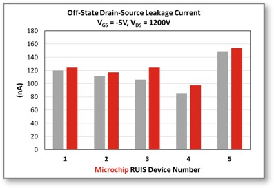
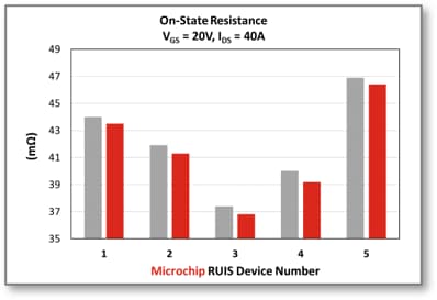
We observe that three of the four MOSFETs survived RUIS quite well. However, the mSiC MOSFET is in a class of its own when we look at the TDDB for Microchip and three other SiC MOSFET suppliers. For each case, we measure TDDB before UIS and another following 100,000 pulses.
Looking at only our devices, we see unparalleled stability in both RDS(on) and drain-source leakage, indicating that our mSiC MOSFETs are indeed ruggedized to avalanche and able to safely ride through the most demanding electric overstress conditions.
 |
 |
 |
Short-Circuit Capability
Short-circuit capability allows the device to withstand high currents without damage. During a short circuit, the current through the device can increase to exceedingly high levels, which can cause the device to overheat and fail. SiC MOSFETs have a much higher short circuit capability than silicon MOSFETs, allowing them to withstand higher currents without damage. This is important for applications where there is a risk of a short circuit and for applications where there is a high demand for current, such as in Electric Vehicles (EVs).
The short-circuit capability of a SiC MOSFET is measured by the short-circuit current, which is the maximum current that the device can withstand without damage. The short-circuit current of SiC MOSFETs is typically much higher than that of silicon MOSFETs. This is because the SiC MOSFETs are made of a material that is more resistant to damage from high currents.
Short circuit withstand time is a measure of how long the MOSFET can survive the DC link being suddenly shorted across the drain-source terminals. In short circuit, the MOS channel is enhanced, meaning the overstress surge is shared uniformly across the die.
When testing a production-grade 700V, 35 mΩ mSiC MOSFETs at various DC voltages and gate voltages, we see that for a 350V DC link, the device can safely ride through 10 µs of short circuit time at VGS = 20V. Even at a 560V DC link, the 700V MOSFET can live through 3 µs of short circuit time, which is more than enough time for control schemes to come to the rescue.
 Short circuit emulates the application condition of shorting the MOSFET’s drain-source across the DC link. |
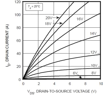 Cells are enhanced (MOSFET is ON); peak current intended to distribute uniformly across die. |
Neutron Susceptibility and FIT Rate
SiC devices are also more resistant to radiation damage than silicon devices because SiC has a higher density of electrons than silicon, making it more difficult for radiation to affect the electrons in the atoms. Neutrons can degrade or damage system performance at or above sea level. Tests show that SiC MOSFETs exhibit 10× lower Failure in Time (FIT) rate than comparable silicon IGBTs at rated voltage.
Tests of SiC products from several vendors also showed mSiC MOSFETs perform well against SiC competition with respect to neutron irradiation. This makes SiC a logical choice to use in applications like EV chargers, on-board chargers and power suppliers that specify operation to an elevation such as 4000m to 5000m.
 SiC MOSFETs have 10× lower FIT rate than comparable silicon IGBTs at rated voltage. |
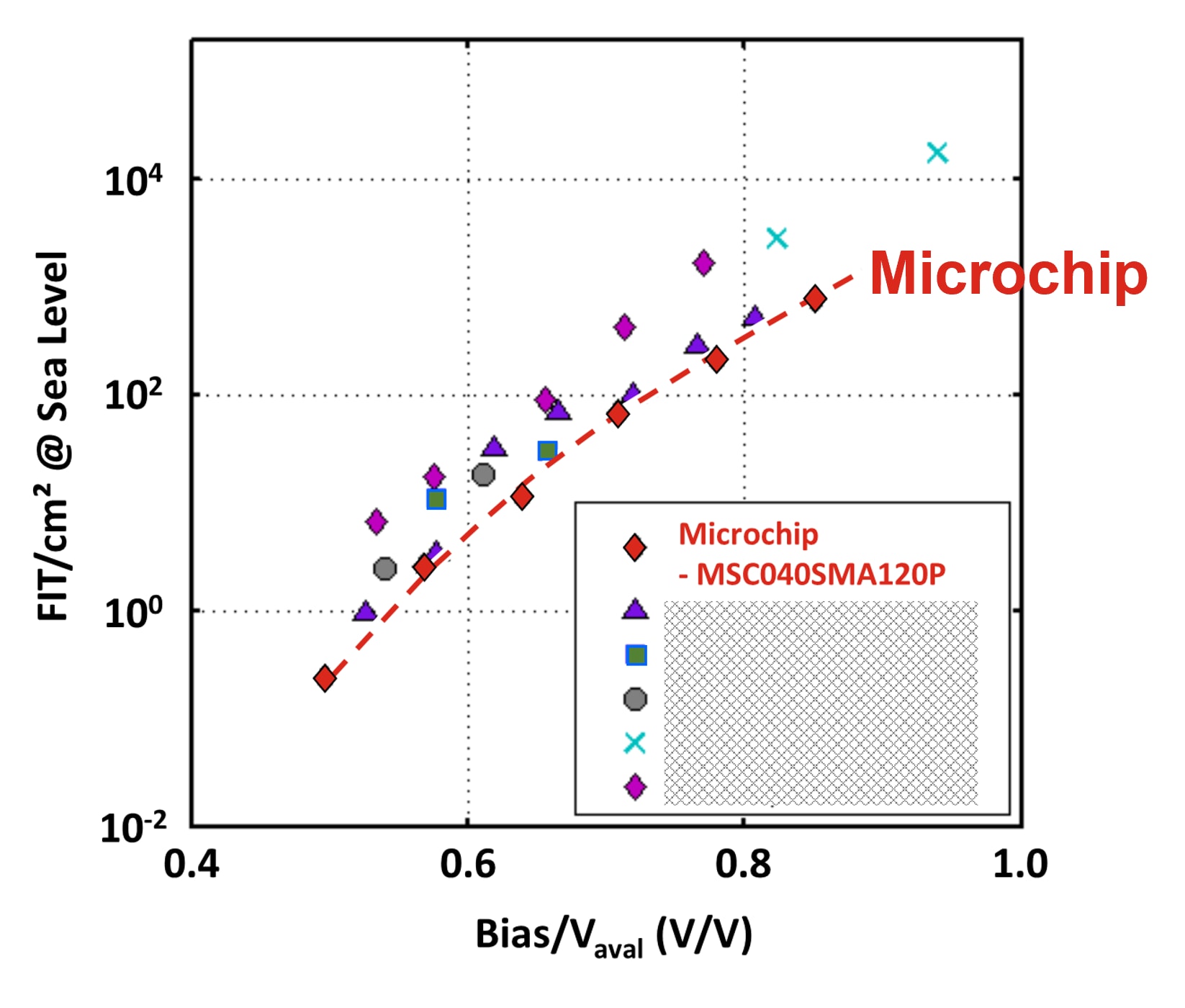 Microchip SiC MOSFETs perform well against SiC competition with respect to neutron irradiation. |
RDS(on) Versus Junction Temperature
The relationship between RDS(on) and junction temperature is important because it affects the overall performance of the circuit. The RDS(on) curve is a good indication of ruggedness because it indicates how well a device will perform. The circuit will not be able to perform as expected if the RDS(on) is too high.
 VS Junction Temp MRT364372") |
Low RDS(on) helps a device withstand high temperatures and voltages, allows it to switch quickly and efficiently and helps the device withstand harsh environments. A low RDS(on) can also improve the efficiency of the circuit: the lower the RDS(on), the less power is lost in the MOSFET.
Understanding the relationship between RDS(on) and junction temperature is also important because it can help to choose the right MOSFET for an application. If the junction temperature that a MOSFET will be exposed to is known, you can choose a MOSFET with a low RDS(on) that can withstand that temperature. This will help you to ensure that your circuit performs as expected.
A flatter RDS(on) curve over temperature means the SiC MOSFET device will have greater stability in conduction losses over a larger temperature range, allowing the designer to maintain a tighter margin for thermal management.
Start Designing with SiC
Getting started with designing with Silicon Carbide (SiC) involves understanding its benefits and applications. We offer a range of Silicon Carbide (SiC) power products which are the key to faster, more efficient energy solutions. We recommend reviewing our SiC MOSFET Design Recommendations and our Driving mSiC MOSFETs application notes.
We also provide comprehensive support for SiC design-in process including extensive documentation, design tools, SiC reference designs and technical support to help designers in their product development.