Enhance Your Radio Frequency Applications Using a Digital-to-Analog Converter
Having the ability to accurately control a bias voltage can help to optimize the performance of tuning circuits in a range of Radio Frequency (RF) applications. A Digital-to-Analog Converter (DAC) is ideal for this purpose, making it a useful addition to RF designs.
Using LDMOS In RF Applications
Many RF power amplifier applications, including GSM and CDMA cellular base stations, radar, CATV and portable radio devices, use LDMOS transistors. However, due to a build-up of charge in the drain-gate region, quiescent current (IDQ) for a fixed-gate bias voltage (VGS) can drift significantly over temperature. The change in IDQ is proportional to both gate bias voltage and temperature. To maintain the maximum output power while maintaining high linearity, IDQ must be maintained at a constant value across the full operating temperature range. To achieve this, the gate bias voltage requires adjusting during operation to compensate for changes in temperature. For these applications, a DAC like the MCP4716 or MCP4726 can be used as part of the bias control circuitry to set IDQ with ±4% accuracy.

Variable Capacitance
Some simpler RF circuits use a varactor diode (or varicap) with an adjustable capacitance that varies in response to the applied voltage. These devices are often used for tuning circuits, such as RF oscillators and filters found in applications such as wireless microphones and radios. A reverse bias voltage creates a depletion zone around the P-N junction, the thickness of which determines the effective capacitance of the diode. The thickness of the depletion region changes in response to changes in the reverse bias voltage which can therefore be used to adjust the capacitance of the device.
Varactor diodes are specified with a nominal capacitance value and the capacitance range that can be achieved between minimum and maximum voltage levels.
A DAC provides a convenient, cost-effective way to adjust the bias voltage of the varactor, but it has the potential to introduce sources of error that can cause an undesired shift in the capacitance of the device. The primary sources of error that should be considered include:
- Varactor nonlinearity
- Offset errors
- DAC Integral Nonlinearity (INL)
However, these errors can be accounted for when programming the microcontroller used to set the DAC output voltage.
Preventing Unwanted RF Modulation
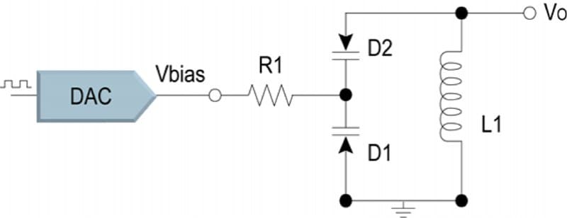
Another potential problem is RF modulation of the bias voltage due to an induced voltage signal from an external noise source (like an antenna in the system). The LC-Tank circuit portion of a voltage-controlled oscillator is used for FM modulation in the wireless microphone or radio.

Here, a back-to-back varactor configuration helps to minimizes the effects of unwanted RF modulation. If an undesired external signal is injected into the circuit, the bias across one varactor diode increases as the other decreases, thereby keeping the overall capacitance unchanged. Note that by placing two varactors a in a series configuration, the overall capacitance is halved. To prevent RF signals from affecting the circuitry outside the tuning circuit, the bias voltage is fed through an isolation resistor or an RF choke.
DAC Advantages
There are other benefits to using a DAC to bias a varactor diode. A multi-output DAC can be used in a multistage application, for example, with three of the four channels in a four-channel DAC being used to provide low-, mid- and high-frequency filtering. The fourth channel remains available to provide offset voltage calibration elsewhere in the circuit (or can simply be powered down if not required). This eliminates the requirement to set up separate biasing schemes, thereby saving board space and reducing design time.
Some DACs, for example the MCP4728, also include nonvolatile memory in which configuration data, such as output voltage levels and channel status (on/off) can be stored. The allows the device to be reset or powered up in a preprogrammed tuning configuration state. This state can then be recalled at power up (after an outage) or if a desired event or a recognized set of inputs occur.
You can read more about this type of solution in AN1326: Using the MCP4728 12-bit DAC for LDMOS Amplifier Bias Control Applications. If you would like more information about how DACs can be used in your designs, please visit the Digital-to-Analog Converter page on our website.
MCP47FXBX4/8 Data Sheet: 8/10/12-bit Quad/Octal output, with I2C interface.
MCP48FXBX4/8 Data Sheet: 8/10/12-bit Quad/Octal output, with SPI interface.
MCP48CXBXX Data Sheet: 8/10/12-bit Single/Dual output, with SPI interface
