
Digitally-Enhanced High-Speed ADCs for Low-Power Wireless Applications
Digitally-enhanced high-speed ADCs can help simplify today's radio frequency (RF) system designs and allow for lower overall power operation. digitally-enhanced, high speed pipelined (200/80 Msps) analog-to-digital converters (ADCs) come with many configurable digital signal post-processing options.
Today’s digital radio architectures rely heavily on advanced digital signal processing technologies, such as Digital Down-Conversion (DDC) for In-phase and Quadrature (I/Q) signal detection and digital decimation filtering for improving Signal-to-Noise Ratio (SNR). DDC and many other digital processing functions are usually implemented by digital building blocks that require extensive firmware operations using Field Programmable Gate Arrays (FPGAs). Figure 1 shows an example of a software-defined radio receiver employing a super-heterodyne, dual-stage conversion architecture, which is very common in radio frequency (RF) communication systems and high-speed data acquisition systems.
Firmware development for Digital Signal Processing (DSP) building blocks is a very time-consuming task for most system developers. An FPGA also tends to be the highest-cost component in many systems. In order to reduce overall system hardware requirements, complexity, development time and cost, a digitally enhanced Analog-to-Digital Converter (ADC) with built-in Digital Signal Post-Processing (DSPP) option is an excellent solution to meet today’s rigorous design requirements.
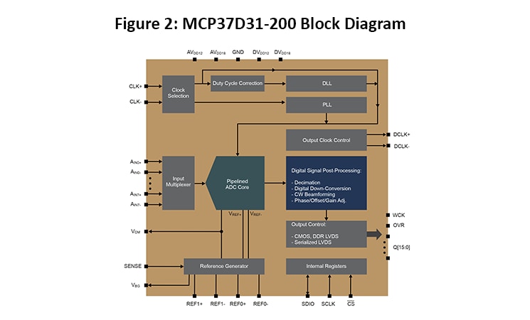
As shown in Figure 1, the conventional ADC and DDC block can be replaced with a digitally-enhanced ADC, which can output I/Q signals or up-converted real signals. The MCP37Dx1-200/80 are digitally enhanced, 16/14/12-bit, low-power, 8-channel MUX, 200/80 Msps ADCs with SPI Serial Interface, capable of performing variety of DSPP functionalities. Using digitally-enhanced ADCs eliminates the need for extensive FPGA-based logic in low-power, wireless applications.
Microchip’s MCP37D1-200/80 ADCs also feature built-in decimation filters for improving SNR, Fractional Delay Recovery (FDR), phase/offset and gain adjust of individual channels. In addition, they come with built-in ADC linearity calibration algorithms such as Harmonic Distortion Correction (HDC), DAC Noise Cancellation (DNC) and Dynamic Element Matching (DEM). Available in 12-, 14- and 16-bit versions, this family of pipelined ADCs also deliver some of the lowest-power operation in the industry. Its power dissipation at 200 Msps is 436 mW with CMOS digital I/O, 490 mW with LVDS digital I/O and 390 mW without digital I/O.
Microchip’s family of high-speed pipelined ADCs is well suited for a variety of applications, including low-power portable instruments, cellular base stations, ultrasound and sonar imaging and more. If you want to simplify the development of your low-power wireless application, learn more at our Analog-to-Digital Converters Products page and ADC Products Parametric Chart.