Best of Two Worlds: Small Footprint FPGA and Cost-Effective PCB Technology
Learn about the possibility to combine small FGPA packages with cost-effective PCB technology for space-constrained applications.
Is your electronic design space-constrained? Need to get into a small housing but still have a lot of functionality? And is the PCB technology of cost-concern?
Yes? Good. We should talk, so read on.
The story starts with having a low-power FPGA to fit your design. The Microchip Flash-based PolarFire® FPGA is this device, it is designed to typically work without any heat sinks, also at high ambient surrounding temperature. PolarFire also has an older sibling, the Igloo2 and SmartFusion2 FPGA and SoC where the low-power topic also applies.
I am not going into details about the FPGA itself in this article but will look at the package story. For details of PolarFire, please have a read here.
Looking at the product table of PolarFire the package story looks pretty harmless. Some readers my even shy back because of the pitch size of 0.5 mm.

This is where the beauty starts. The FCSG325 package is built on 0.5 mm pitch, yes, however it also has several white spaces on the ball grid array:
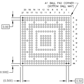
The inner area of the package is populated with pins for supply and ground, the outer rings are user IOs and transceiver pins. This means, routing out user signals is only through a small part of the package.
Several use cases where put onto this package and layed out as examples:
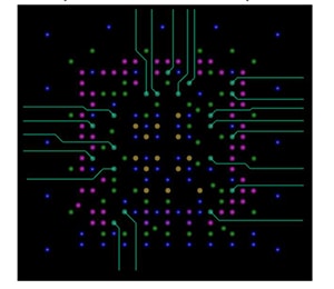
1) Generic layout for all pins
The top layer is used to route out all IOs from the outer rings, including the transceivers at the bottom of the image. No vias at all are required for these signals.
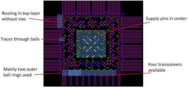
The bottom layer takes signals from the middle ring. As the outer ring was routed without vias no obstacles are present and the signals can be brought out easily. The middle of the package shows vias used for power and ground for their separate layers.
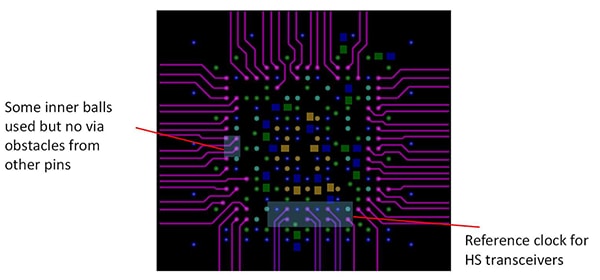
A few pins where left which require a third layer with very few signals to be routed out:
The vias used here are of 0.1 mm, the rest of the layout can be achieved with the typical rules of 0.8 mm pitch. No buried/blind vias were required.
2) DDR4 with 32 bit data-path

The FCSG325-package has two pre-defined suggestions for DDR4 memories which allows a very quick and simple pin allocation inside the FPGA. Is this a drawback of less flexibility or a benefit? Clearly a benefit! Choosing an optimized pin out for DDR4 without any congestion is an interative process. Having the pre-defined layout turned the pin out into a SEP (somebody else’s problem) and can save you layer count and will save time and grey hair.
The DDR4 interface was layout out based on this suggestion and was done in routed based on two signal layers only. These two layers include all 32 data and the address/command-lines. Again, no buried/blind vias had to be used here.
Now, there are circumstances where this suggested layout may not work due to some side constraints. In those cases where you have to divert from the suggested layout Microchip offers the paid service to help you with or check on your layout via design services. Details on this offering can be found on our website.
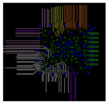
3) Cost-optimized layout
If only the IOs in the outer ring of the package are used, then additional cost optimizations are possible. The image shows several independent interfaces routed outwards on the top layer. This keeps the white space under the package free and allows the use of vias with 0.33 mm diameter.
Zooming in onto the supply pins shows the larger vias in the free white space.
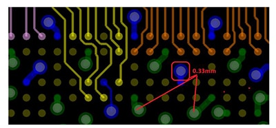
In all use cases the trace widths was at 4 MIL / 0.1 mm and the distance between trace & pad was 3.1 MIL / 0.08 mm.
Layout suggestions for this and other packages are also published online here and here.
In essence, where do these layout suggestions help you and your design? These are pointers showing you how to combine the benefits of the two worlds, small package pitch and cost-effective PCB technology and with that tackle your space constraints.
Stay ahead with the latest hardware trends. Explore how makers are applying these innovations in real-world projects at our Makers page.
Happy designing!