
Microchip’s Analog Tools Ecosystem Part 3: Validating the Design with Mindi
This is a four-part series where we will dive into the analog design tools ecosystem. In this article, readers will explore how to validate their design with Mindi.
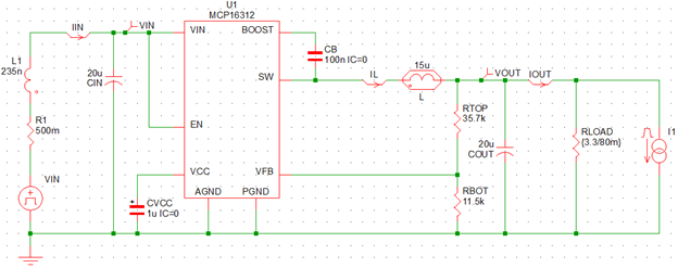
To assist in the design validation phase, Microchip provides the MPLAB® Mindi™ Analog Simulator, which is built upon the SIMetrix and SIMPLIS simulation engines. Continuing from the part 2 article, we had just walked through exporting and downloading the schematic for our IoT platform module power supply. Opening the file in the Mindi simulator reveals the basic schematic below.

In our application, the input source is sometimes connected via a cable, so we’ll add a simple model for that. We’ll also add input current and voltage probes to observe the effect of this cable model on the input module supply as the converter operates. There is no enable signal in this system, so we’ll remove the signal source and tie EN to VIN.
The default load is a static resistor to draw the right output current at the target output voltage. In our application, there is generally a base level of current drawn with periods of higher consumption for functions like communicating over the wireless transceiver. To do this, we’ll change the resistor to a larger value to draw approximately 100 mA in a steady-state condition. We’ll also add a pulsed current source to emulate the wireless transmitter activity during a brief interval, resulting in the schematic below.
After running the transient simulation, a number of graphs are displayed, such as the output voltage and current below. We can see the steady-state draw of 80 mA and the periodic load step starting at 1 ms. The PFM operation in light load (80 mA) can also be observed with its associated increase in ripple voltage.
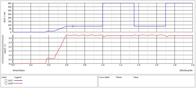
Zooming in on the output voltage, we can better observe the ripple and the regulation during the heavier, 400 mA, load in which the device is operating in PWM. In the steady state PWM mode, the output is regulated to 3.28 V, which is the expected deviation from 3.3 V given standard resistor values. In PWM mode, the output voltage ripple is very small compared to the ripple in PFM mode. The higher efficiency in PFM mode is gained by driving the output to a slightly higher voltage and then discontinuing pulses until the voltage decays back to the regulation point.
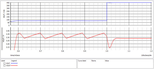
This larger ripple in PFM mode may be a concern for some applications. Remembering back to our comparison chart in MAD, we had a second part choice, the MCP16312, that was nearly identical to the MCP16311, except that it only supported PWM operation. Replacing the MCP16311 with the MCP16312, we can re-simulate and compare the performance in the graph below as both the previous and current simulation waveforms are displayed. Here, we can see that the ripple in light load is the same as when fully loaded, at a cost of some efficiency in the light load condition. We can also see that the step load response is a little better too, as the output voltage dips momentarily to 3.20 V as compared to the PFM case where it drops below 3.15 V before starting to recover.
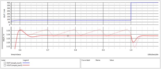
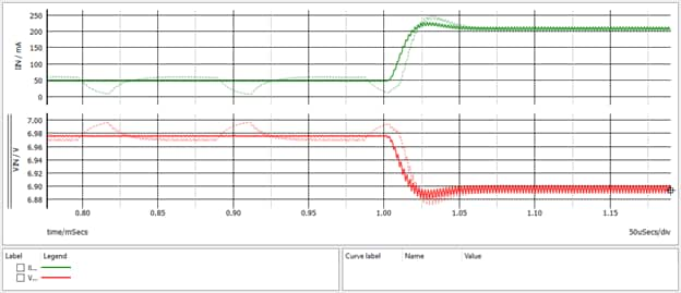
Now that we’re satisfied with the output response, we turn our attention to the input waveforms, as seen below. Here again, both the MCP16311 and MCP16312 waveforms are displayed, since we ran these back-to-back without closing the graphs. In either case, there doesn’t seem to be an issue. We do have a slight drop in the input voltage but not enough to cause a problem with the converter.
Now that we’ve verified the design, it’s time to start the physical design, which we will discuss in part four of this blog series.
Read the other articles in this series:
Part 1: Creating Robust Analog Designs
Part 2: Getting Started with MAD
Part 4: PCB Symbols and Footprints
Connect with Terry Cleveland on LinkedIn.
Connect with Chris Twigg on LinkedIn.