
Microchip’s Analog Tools Ecosystem Part 2: Getting Started With MAD
This is a four-part series where we will dive into the analog design tools ecosystem. In this article, readers will explore how to get started with the MPLAB® Analog Designer (MAD) tool.
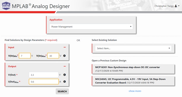
Starting a new power supply design is easy with the MPLAB® Analog Designer (MAD) tool. To help illustrate this process, let’s design a power supply for an IoT platform module that could be embedded within multiple different appliances or pieces of industrial equipment. The module includes a microcontroller, an 802.11 wireless module, several sensors, and some indicator LEDs, all of which are estimated to consume approximately 400 mA from a 3.3 V supply. Since this platform will be used within different end applications, the input supply can be a wide range, from 7 to 30 V.
We begin our search for a solution by navigating to microchip.com/mad and entering our design parameters under the power management application space. The input and output voltages are entered directly from our module requirements, but we have increased the output current capability by 50 percent to give us some margin. We now click the search button to find potential solutions.
After a few seconds, a list of potential solutions will be displayed as seen below. There are several categories of solutions displayed, such as the evaluation boards and custom design generators. We are looking for a custom design that we can drop down on our PCB, so we collapse the evaluation boards category.
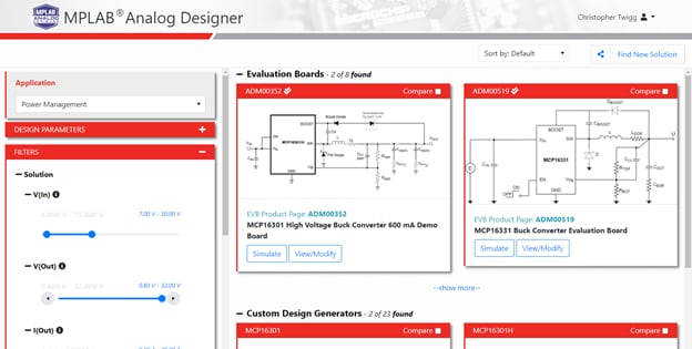
To further reduce the list of possible solutions, we can use the filters in the left-side panel. For this application, we might want to reduce the PCB area needed, so we select the synchronous rectification option under the features filter list. This constrains MAD to suggesting solutions with integrated FETs and reduces our list of custom design generators to 15.
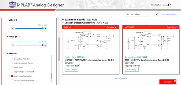
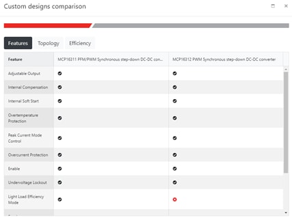
Taking the top two suggestions, we can compare them by clicking the compare boxes in the top-right of each solution window and clicking on the red compare button on the bottom-right section of the screen. The result is the chart seen below, in which it can be seen that the parts are nearly identical, except for the “Light Load Efficiency Mode” feature. The MCP16311 has a PFM mode in addition to PWM mode that allows it to be more efficient than the MCP16312 when the load current is small.
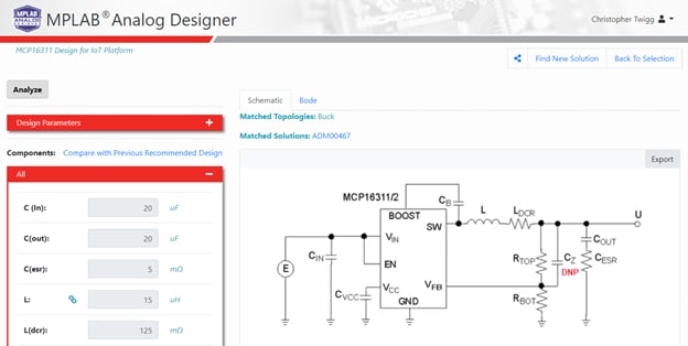
Since the first option (MCP16311) looks reasonable, we click on the start design button to start the design generator tool, as seen in the figure below. A simplified, typical schematic is displayed in the panel on the right, and the design parameters and a list of components are on the left. In many cases, there are more tabs than the schematic that display additional information, such as the Bode tab in this example that displays the gain/phase response of this circuit. The components tab displays the recommendations from the design generator, but the user can override most of these parameters by clicking on the values and regenerating the solution. In this manner, the designer can tweak the schematic and see the effect on the circuit performance in the Bode tab.
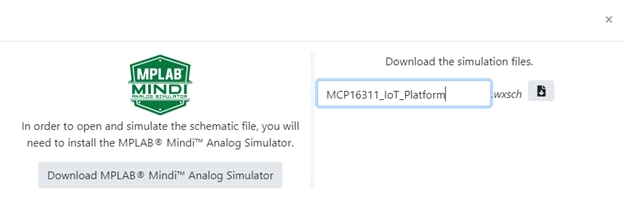
Once the designer is satisfied with the design generator output, he or she can click on the export button in the top-right section of the window to export a schematic file for use within the MPLAB® Mindi™ Analog Simulator. The tool will prompt the user to enter a filename, as seen in the figure below. Once save, the schematic can be opened, altered, and evaluated further using the Mindi Simulator, which is the topic of the next blog post in this series. Keep an eye out for part three on how to validate the design with Mindi.
Read the other articles in this series:
Part 1: Creating Robust Analog Designs
Part 3: Validating the Design with Mindi
Part 4: PCB Symbols and Footprints
Connect with Terry Cleveland on LinkedIn.
Connect with Chris Twigg on LinkedIn.