Exploring a variety of RF circuits including power amplifier applications — such as GSM and CDMA cellular base stations, radar, CATV and portable radio devices as well as RF oscillators and filters found in wireless applications, such as wireless microphones and radios.
There are many aspects to using varactor diodes in RF electronic circuits. The configuration to the varactor circuits can affect their operation – some small variations can lead to major differences in performance.
In view of the fact that RF circuits are not always easy to optimize, it is necessary to ensure the varactor circuits utilize the best methods of driving varactor diodes as well as the most successful basic circuits.
Varactor (or “varicap”) diodes are used primarily in radio-frequency (RF) circuits to provide a capacitance that can be varied by changing the applied voltage. These types of diodes often are used for tuning circuits, such as RF oscillators and filters found in wireless applications like wireless microphones and radios. Designers, then, should know about the benefits of using a nonvolatile digital-to-analog converter (DAC) to provide the biasing voltage of a varactor diode used as a voltage-controlled capacitor.
The varactor diode is operated under reverse bias, which creates a depletion zone around the P-N junction. Changing the level of the reverse bias changes the thickness of the depletion region and, thus, the effective capacitance of the diode. Increasing voltage causes a decrease in capacitance.
Varactor diodes are specified with a nominal capacitance value and the range of capacitance that can be achieved with a maximum and minimum voltage level. Increasing the bias voltage range increases the capacitance range available, but designers can also look for varactors with a larger capacitance-to-voltage ratio.
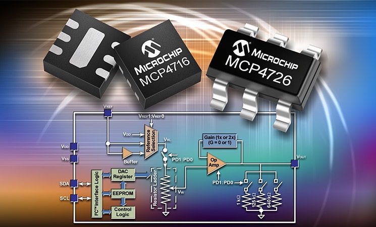
A convenient solution for creating a varying bias voltage is to use a DAC. Most DACs have an output voltage range of 0 V to +5.5 V. If a higher voltage bias is required, though, then a high-voltage DAC can be used. However, it may be more cost-effective to use a low-cost, high-voltage operational amplifier in a non-inverting configuration to provide level shifting of the output voltage from a common 5.5-V DAC.
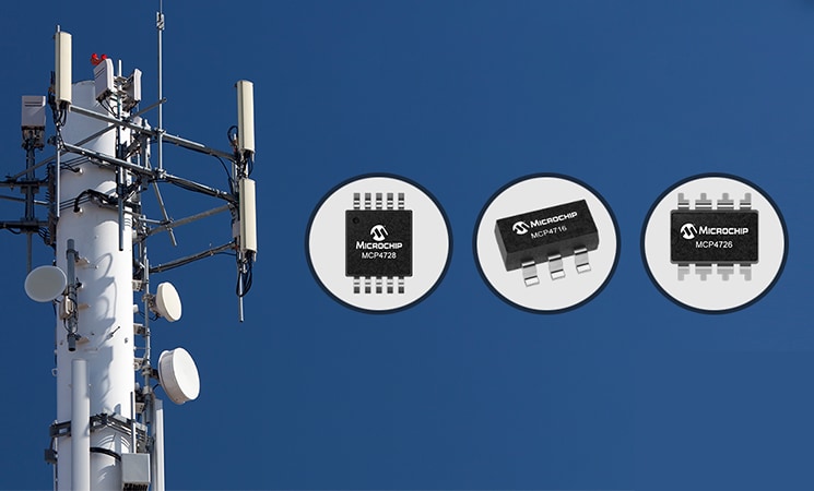
Some RF power amplifier applications – such as GSM and CDMA cellular base stations, radar, CATV, and portable radio devices – use LDMOS transistors. Due to the charge build-up in the Drain-Gate region, however, there can be significant drifts of quiescent current (IDQ) at a fixed-gate bias voltage (VGS) over temperature. The IDQ changes proportionally with both the gate bias voltage and temperature. To maintain the maximum output power with high linearity, the IDQ needs to be constant over time across all operating temperature ranges. To achieve this, the gate bias voltage needs to be adjusted during operation to compensate the temperature changes. In these types of applications, a Digital-to-Analog Converter (DAC) like the MCP4716 or MCP4726 can be used in the bias control circuits to maintain the IDQ within a ±4% range. Read more about this type of solution in AN1326: Using the MCP4728 12-Bit DAC for LDMOS Amplifier Bias Control Applications.
Some simple RF circuits use a varactor, or varicap, diode to provide a capacitance that can be varied by changing the applied voltage. These types of diodes are often used for tuning circuits, such as RF oscillators and filters found in wireless applications, such as wireless microphones and radios.
The varactor diode is operated under reverse bias, which creates a depletion zone around the P-N junction. Changing the level of the reverse bias changes the thickness of the depletion region and, thus, the effective capacitance of the diode. Increasing voltage causes a decrease in capacitance. Varactor diodes are specified with a nominal capacitance value and the range of capacitance that can be achieved with a maximum and minimum voltage level. A DAC can provide a convenient, cost-effective solution for creating the variable bias voltage.
Using a DAC does introduce sources of potential error. The varactor is affected by any form of amplitude variation of the bias voltage, resulting in an undesired shift in capacitance. Deterministic errors can be accounted for when using the microcontroller to program the DAC output voltage.
The primary sources of error that should be considered include:
• Varactor nonlinearity
• Offset errors
• DAC Integral Nonlinearity (INL)
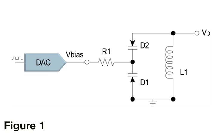
RF modulation may also be caused by voltage induced from a noise source—perhaps from an antenna in the system. Figure 1 shows an LC-Tank circuit portion of a voltage-controlled oscillator. This circuit allows for FM modulation in the wireless microphone or radio. Here, a back-to-back varactor configuration minimizes the effects of RF modulation. If a varying signal is injected, the bias across one diode increases as the other decreases, thus keeping overall capacitance unchanged. Note that the two diodes are in series with each other, so capacitance is half of a single varactor set-up.
To prevent RF signals from affecting the circuitry outside the tuning circuit, the bias voltage is fed through an isolation resistor or a RF choke.
There are other benefits to using a DAC to bias a varactor diode. For example, multiple output-channel DAC devices can be used in a multistage application. Or three channels in a four-channel DAC could potentially be used for separate band-pass filters for low-, mid- and high-frequency filtering. The fourth output could be used for offset voltage calibration elsewhere in the circuit or be turned off when not in use. This eliminates the need to set up separate biasing schemes, which saves board space and reduces design time.
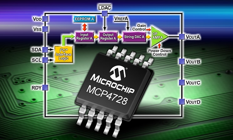
Some DACs, for example the MCP4728, offer nonvolatile memory. This enables configuration data, such as output-voltage levels and channel status (on/off), to be stored in the DAC’s on-board nonvolatile memory. The device can then be reset or powered up in a known state, which could allow a pre-programmed tune to be stored. This tune can be recalled when a desired event or input occurs, or when power is lost and restored.
There are other benefits to using a DAC to bias a varactor diode. For example, multiple-output-channel DAC devices can be used in a multistage application. Additionally, in a four-channel DAC, three channels could potentially be used for separate band-pass filters for low-, mid-, and high-frequency filtering. The fourth output could be used for offset voltage calibration elsewhere in the circuit, or it could be turned off when it isn’t in use. Space and design time can be saved by avoiding having to set up separate biasing schemes.
Some DACs such as the MCP4728 also offer on-board nonvolatile memory, which can store configuration data such as output-voltage levels and channel status (on/off). This enables the device to be reset or powered up into a known set state, which could allow a pre-programmed tune to be stored. The tune could be recalled when a desired event or input occurs or when power is lost and restored
For more information about using DACs in your design, please visit our Digital-to-Analog Converter page.