ADC Parameters
Since every application is different, and design priorities dictate which
parameters are most important, the search features of MAPS are utilized to
select the best ADC for a given set of design requirements. The major ADC
parameters are captured in this data base, allowing the user to quickly narrow
a Microchip ADC search to the best few selections. Here is an overview of the
Search Parameters:
Architecture - SAR, Delta-Sigma, Dual Slope – The SAR
converter uses a capacitive array at the analog input. This capacitive array
and the remainder of the device are easily manufactured in a CMOS process,
making it easy to integrate it with microcontrollers or microprocessors. The
Delta-Sigma converter is an oversampling system that uses feedback and noise
shaping to improve noise performance and increase resolution. The Dual Slope
converter uses a rising and falling ramp of a known rate & measures the
time for the ramp to "cross" the input signal.
Resolution – The number of possible output bits an A-D
Converter can produce in one conversion.
Digital Interface – SPI™ is a three or four-wire interface.
With this interface the chip is slave device that is selected with a CS pin.
I2C™ is a two-wire Philips standard interface.
Sample Rate – The speed that a converter can continuously
convert several conversions. Typically specified as samples per second (sps) or
Hertz (Hz)
Single-ended inputs – An A-D Converter that is configured for
one input voltage that is referenced to ground. Pseudo-differential inputs are
considered single ended for this program.
Differential Input – the A-D Converter has two inputs per
channel. These inputs subtract or differential the input signal.
Pseudo-differential inputs are considered single ended for this program.
Voltage reference (also know as analog voltage reference) – The
input range (VIN) and LSB sized is determined by the voltage
reference (VREF) to the converter. Depending on the converter, VIN
= VREF or VIN = 2VREF. LSB = VREF /
2n or LSB = 2VREF / 2n (were “n” is the number of bits).
VDD (min/max) - The VDD Voltage is the
specified supply voltage of the deivce, and represents the voltage between the
VDD and VSS pins. Typically, VDD is the system
voltage and VSS is the system ground.
Internal buffer – The A-D Converter input has a high impedance
input that “isolates” the input signal from the converter.
Differential Non-Linearity (DNL) – The maximum deviation in
code width from the ideal 1 LSB (FS/2n) code width. The difference is
calculated for each transition. This is illustrated in Figure A.2 where
the ideal transfer function is a solid line and the DNL error is a dashed line.

Figure A.2. The differential nonlinearity is the difference
between an ideal code width and the measured code width.
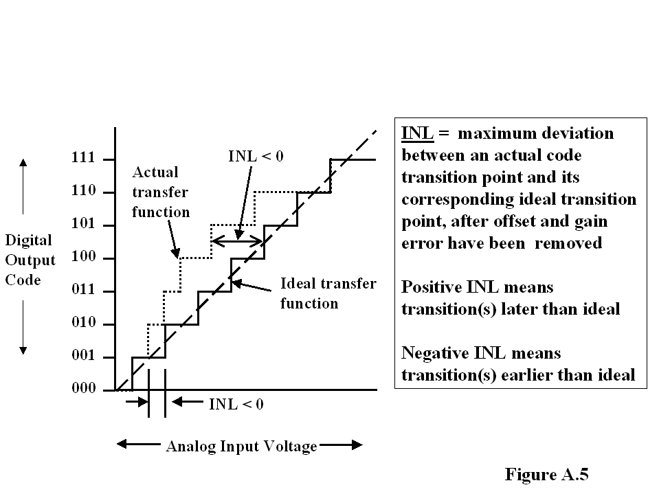
Integral Non-Linearity (INL) – The maximum
deviation of a transition point from the corresponding point of the ideal
transfer curve with offset and gain errors zeroed. See Figure A5.
No Missing Code – Implies that an increase (or decrease) in the
analog voltage input will always increase (or decrease) in digital output
converter code. A converter with no missing code is also monotonic.
Effective Number of Bits (ENOB) - The units of measure for
SINAD is dB and the units of measure for ENOBs is bits. SINAD can be converted
to ENOB with the following calculation: ENOB = (SINAD – 1.76)/ 6.02
Signal-to-Noise Ration plus Distortion (SINAD) is the calculated combination of
SNR and Total Harmonic Distortion (THD). SINAD is the ratio of the RMS
amplitude of the fundamental input frequency of the input signal to the RMS sum
of all other spectral components below one half of the sampling frequency
(excluding DC). The theoretical minimum for SINAD is equal to the SNR or 6.02n
+ 1.76dB.
Package - This column lists the available package types for a
given device. Industry standard nomenclature is used when possible, although
some manufactures have packages that are unique.
Pinout – This column lists a unique 5 digit code for every
package variation, allowing the various pinouts for a given package to be
compared. The code is formatted as follows: aa bb c Pkg #pin pinout.
A code match between devices indicate a pin-for-pin match for a given package
type.