The MPLAB® PowerSmart™ Digital Control Library Designer (DCLD) is a tool within the MPLAB PowerSmart Development Suite. The DCLD encompasses the design of the digital feedback loop and code generation rather than the design of the power stage. It allows you to graphically design discrete compensation filters from the first to the sixth order (1P1Z to 6P6Z). Analysis results on timing, number accuracy, resolution and support of alternative fixed-point or floating-point number scaling options help to tune and optimize the final Switched Mode Power Supplies (SMPS) controller firmware for your specific needs.
The core features of the DCLD include:
- Design support for z-domain compensation filters
- Fixed-point and floating-point DSP library generation
- Graphical feedback loop compensation filter adjustment
- Transfer function export
- Built-in number resolution analysis and optimization
- Graphical execution of timing analysis
- ANSI C/DSP assembly code generation
- Support for user code extensions
- SMPS-specific real-time control features such as adaptive loop gain tuning or gate drive optimized anti-windup features

- Main Window
- Feedback Loop Design
- Execution Timing
- Block Diagrams
- Code Generator Output
- MPLAB® X IDE Project Assignment
The main application window is divided into four sections as shown in the figure below. We designed the Graphical User Interface (GUI) according to the UX guidelines for Microsoft® Win32 to make it as intuitive as possible. At the top of the window, you will find menus giving access to files and application functions. A command bar gives quick access to the most common functions of the application.
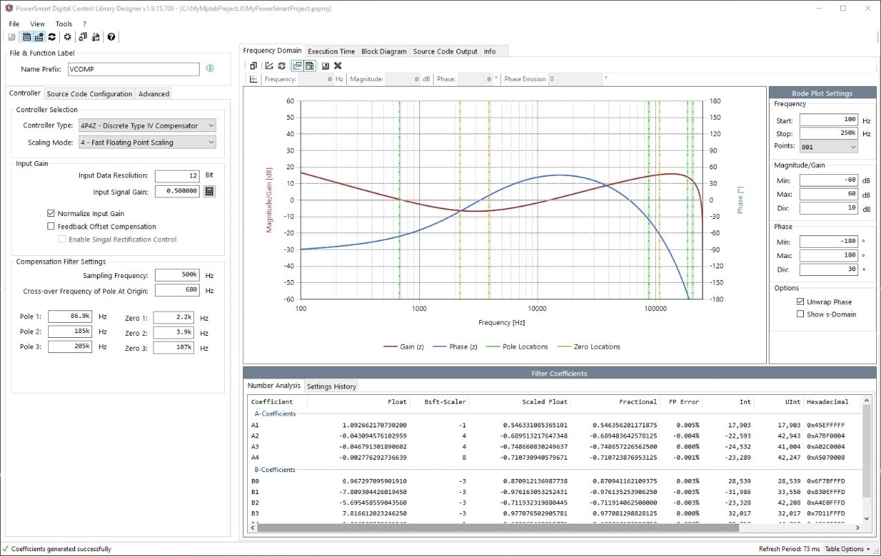
The main section of the window is divided into a user configuration section on the left where you can configure all user settings. On the right, an application output section shows the results of the most recent user configuration. Due to the complexity of digital compensator design, the results are split into multiple sub-sections grouped by topics (frequency domain, time domain, block diagram and source code).
The z-domain controller configuration window is ordered into a left configuration plane and a right plane that shows the results based on the most recent settings. Both planes are separated in individual sub-planes (tabs) offering access to the settings of individual, functional blocks. The default view starts with the controller selection and frequency domain configuration on the left and the Bode plot graph of the transfer function on the right. Below the Bode plot, a data table shows the derivation transcript of the calculation result. This table can also display warnings of the number accuracy analyzer.
Loop tuning is a major step in the design process of any power supply. System optimizations might require you to frequently modify filter settings to solve design tradeoffs. To simplify the management of optimization iterations, the frequency domain view also provides access to the workflow history of the filter design process. This history table captures filter settings when code is generated, assuming generated code will be programmed into a device and measurements/bench tests are performed.
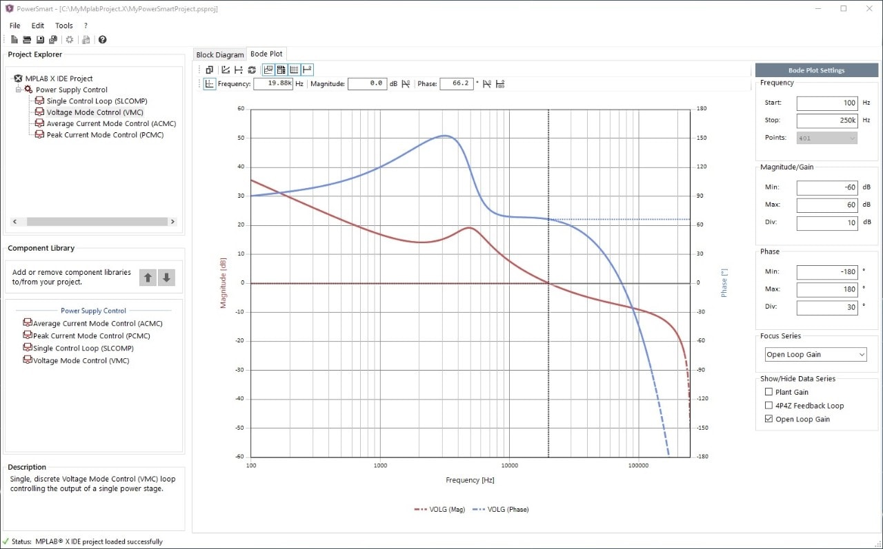
The feedback loop design in DCLD is based around the frequency domain configuration of the compensation filter required to meet certain stability and performance criteria of the power stage. Each filter design, therefore, must be adjusted to the given plant transfer function of the power stage. The combination of multiple transfer functions and calculation of the final open-loop gain in the closed-loop system takes place in the main application of MPLAB PowerSmart Development Suite. You can load different system block diagrams of single- and multi-phase converters with single or cascaded multi-feedback loop controllers, where each partial transfer function can be individually defined and configured. During this design step, the frequency domain view of DCLD provides the data to set up the feedback loop gain characteristics.
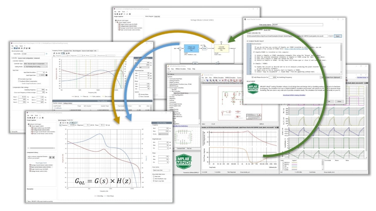
Once all partial transfer functions are defined, the control designer view of MPLAB PowerSmart Development Suite calculates the total open loop gain in the closed loop system and displays the results in a Bode diagram, where cursors are used to analyze stability and performance criteria. Both the plant definition dialog and DCLD can remain open, allowing you to tune the open loop gain in real time without having to switch between different windows or views of the application.
A robust control loop must be executed with a fixed sampling frequency and minimum time delay between an ADC sampling event and the related controller response write-back. Considering the time required to execute the control loop and its repetition rate, each control loop consumes a certain amount of the total available CPU bandwidth. Solving the tradeoff between available CPU resources, control features and control accuracy is a major design challenge.
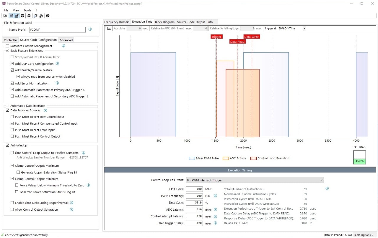
In this context, a proper timing analysis is vital to prevent timing conflicts and CPU load bottlenecks, which both contribute to the risk of major system failures. The execution time chart provided shows the simplified PWM signal (main PWM pulse only), ADC trigger event, ADC conversion period, control loop execution time, controller data read event and controller response write-back event. Any change to selected control features, number resolution and filter type will automatically update the timing diagram, always allowing you to review the impact of a certain feature configuration on the available CPU resources.
The block diagram overview shows four different block diagrams:
- NPNZ controller block
- Compensator block (core block of NPNZ controller block)
- S- to z-domain transfer function
- Compensator processing workflow block diagram
DCLD generates code modules providing a “black box” controller with one unified Application Programming Interface (API). The look and feel of the generated code blocks is like working with hardware peripherals on any MCU where the user sets the configuration and then enables the module. Once these code modules have been added to a project and the user configuration has been added to the firmware, user settings will remain valid even if controller options change, filter settings are modified or even if compensators of different order or different number scaling types are selected.
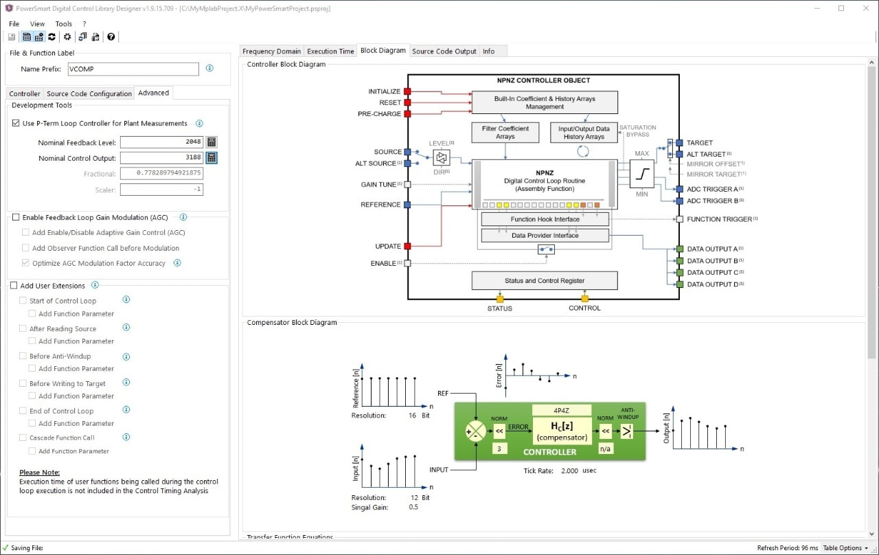
The functional diagrams on this view provide more information about the filter type used and its mathematical form to support a better understanding of the code underneath.
The built-in code generator of DCLD updates the generated source code in real time while you make changes to configurations. The generated code is displayed in individual, separated output windows for assembly and C-code modules where you can edit and review the code.
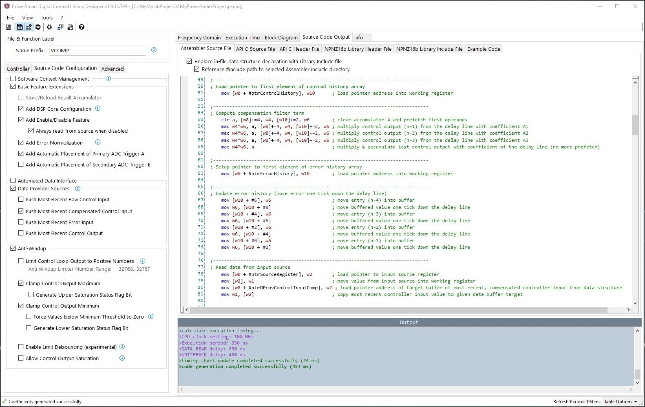
The source code view covers multiple sub-windows for every generated code module. The generated control library source code includes four different files:
- C-source file that contains the static default set of filter coefficients, number scaling constants and the data structure initialization function of this individual controller
- C-header file that holds all public variable and function declarations of this individual controller, making them accessible from throughout the user firmware
- Library C-header file that contains all generic declarations of the NPNZ16b_t data structure, status bits and related global defines. This file is only required once per project. All declarations covered by this library header file will be used by all individually configured controllers.
- Optional library include file that contains assembly references to the generic declarations of the NPNZ16b_t data structure, status bits and related global macros declared in the library C-header file. This file also only needs be added once per project.
Optimized Assembly Code
All runtime functions are generated as optimized assembly routines. These routines read data from and write data to a data structure (NPNZ16b_t), which holds all parameters and pointers to Special Function Registers (SFRs) and user-defined variables used by the library. This data is loaded into the data structure by the C-domain initialization function. Depending on the selected code generator options, additional information will be written to the data structure, from which C-domain application code can gain access (e.g., status bits, most recent calculation results and more).
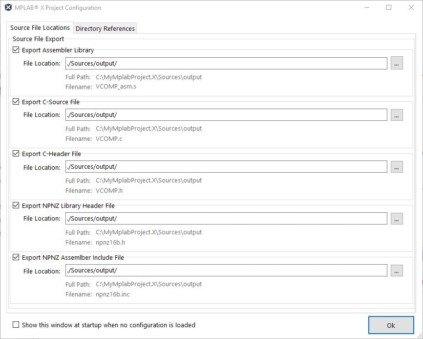
When configuring a control loop library using DCLD, we recommend assigning an MPLAB X IDE project to the configuration. DCLD will then read the project configuration, deriving all the information necessary to provide and pre-select options for the controller device and compiler options set in the user project.
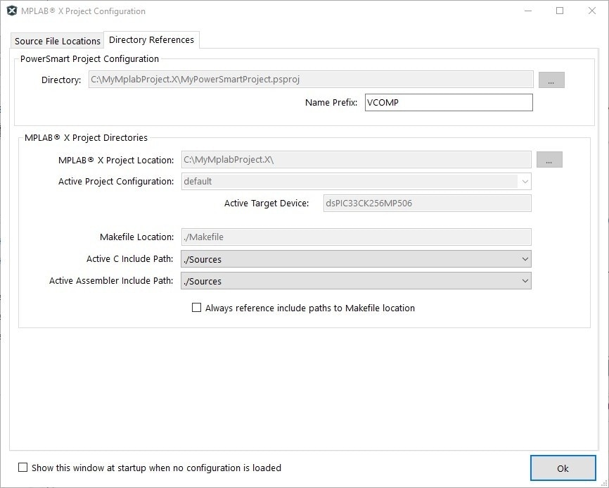
The code generator also places the generated source code files at user-defined locations to not interfere with the user source code structure and source code management.
By default, all source code files will be generated in the root directory of the assigned MPLAB® X IDE project. You can use the project configuration dialog to declare the individual file locations as desired, including network drive locations in team environments.