Assembly and Packaging Key Technologies
Innovative Semiconductor Packaging Technologies
Would You Like More Information or a Quote?
Microelectronics Assembly Services
Our cutting-edge sub-assemblies are created using state-of-the art ECAD and MCAD simulation and design tools. We partner with you to provide world-class products that meet your specific Size, Weight and Power (SWaP) requirements. They are available as digital, mixed-signal, Radio Frequency (RF) and microwave assemblies in rigid and flex rigid substrates.

Capabilities
- Wafer probe
- Wafer sawing
- Die attach
- Wire bonding
- Wedge
- Ball bonding
- Flip chip
- Encapsulation
- Dam and fill
- Large panel over-molding
- Glob top
- Surface mount assembly
- Standard and reducing gas flow
- Labelling, laser marking and serialization
- Burn-in
- Test
Markets and Industries
This technology is suitable for, but not limited to, these markets:
- Industrial
- Security
- Communications
- Medical
Key Benefits
- Scalable manufacturing process
- Customized automated processing for high production volumes
- Component traceability and planning
- Rapid prototyping
- Full supply chain management
Miniaturization Services Using SiP Technology
Our embedded System-In-Package (SiP) technology provides unparalleled miniaturization in a proven and robust package capable of meeting the most stringent quality requirements.
We have developed a technology for embedding components between PCB laminations that enables them to occupy a near-zero area. This allows you to reduce the size of your device or maintain its size while delivering additional functionality.

Capabilities
- Flip chip, wire bond or packaged part
- 3D die stacking
- Low tooling cost
- Inbuilt RF screening
- Internal interconnect
- Custom package design
- Compatible with MIL standard for implantable devices
Markets and Industries
This technology is suitable for, but not limited to, these markets:
- Medical
- Security
- Military
- Industrial sensing
Key Benefits
- Increased security against counterfeiting
- Reduced signal path loss
- Robustness against vibration
- Highly reliability
- Adaptable package to meet your board requirements
- Scalable manufacturing process
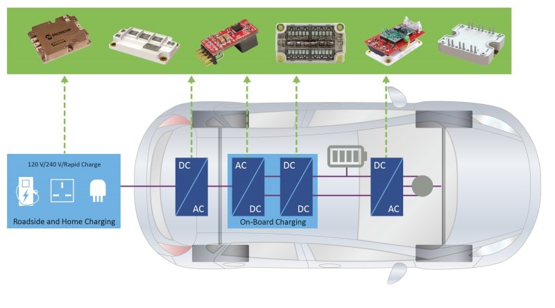
Complex Power Module Services
We design and build a wide range of power modules with superior characteristics such as low stray inductance values and fast switching times using Si IGBT and SiC MOSFET technologies.
These characteristics significantly improve system power density and integration area, making our power modules suitable for the most demanding applications.

Capabilities
- Heavy-gauge wire/ribbon bonding
- Silicone potting
- Film-assisted molding
- Silver sintering
- Module miniaturization
- Direct die bonding
- Tab welding
- Low-/no-void solder
Markets and Industries
This technology is suitable for, but not limited to, these markets:
- Industrial
- Automotive
- Aerospace
- Medical
Key Benefits
- High reliability
- Very fast switching
- High efficiency
- High power density
- Small size for improved system integration
- Module customization
- Intelligent power modules via integrated gate driver
Large Area Panel Molding
As a design alternative to standard injection molding, our Large Area Panel Molding (LAPM) service provides a low cost of entry, fast turnaround and flexible package size.
Another key benefit of LAPM is that it uses thermally matched materials, which allows the same material to be used for the substrate and overmolding to minimize stress throughout the package during thermal cycling.

Capabilities
- Compatible components can be embedded
- Thermally matched package materials
- Internal interconnect—bare die (flip chip or wire bond)
- SiP, BGA, SMT components
- Custom package design
Markets and Industries
- Medical implants and wearable devices
- Sports and fitness
- Security
- Industrial
Key Benefits
- Low cost of entry as there is no expensive tooling
- Fast turnaround time comparable with the standard PCB process
- Flexible size and shape; the large panels allow for economic and scalable production at any package size
- Component traceability and planning