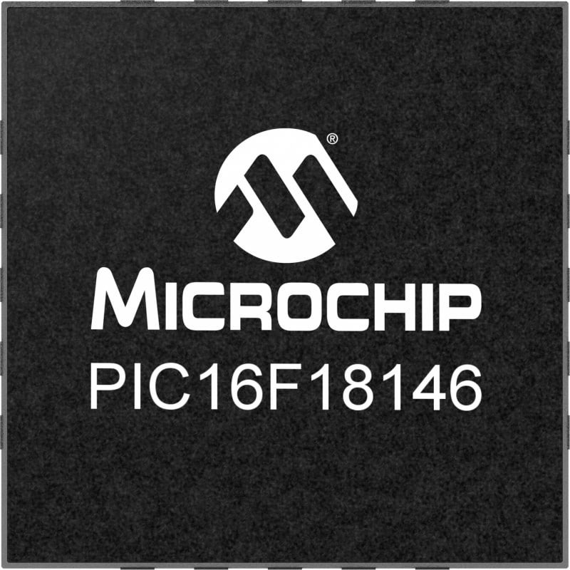
Compact MCUs for Sensor Fusion
The PIC16F18146 series of MCUs leverages a lean toolkit of Core Independent Peripherals (CIPs) to enable size-constrained, sensor-heavy designs. With a 12-bit differential Analog-to-Digital Converter with Computation (ADCC), two 8-bit Digital-to-Analog Converters (DACs) and several communication protocols, this family allows you to mix and match various sensor types without having to add additional hardware to your design. This product family’s ability to both process data and interface with sensors positions these MCUs to act as companion MCUs in more complex systems. Available in 8- to 40-pin packages while also coming in a variety memory options, these small form-factor MCUs can support a wide range of applications such as home automation, industrial process control, automotive and Internet of Things (IoT). If you need the same level of MCU performance with additional analog features, the PIC16F17146 family is an ideal solution.

System Features
Configurable Analog
12-bit ADCC, 8/10-bit DAC and ZCD
The intelligent Analog-to-Digital Converter (ADC), high-speed analog comparators, multiple DACs and a Zero Cross Detect (ZCD) peripheral offer a high level of analog integration for amplification, filtering and signal conditioning for sensing and measurement applications. With the 12-bit differential ADCC, you can achieve high-resolution ADC conversions with strong noise rejection and automated analog signal analysis and data acquisition functions for enhanced real-time system response.
Layout Flexibility
Peripheral Pin Select (PPS)
PPS provides ultimate flexibility when routing digital signals to device pins. With PPS, you can connect any digital peripheral to any I/O pin on the fly for a customized layout. This allows you to maintain layout compatibility with older PIC® MCUs, even as new features are implemented.
Hardware Customization
Custom Logic and Interconnections
You can easily customize the configurable peripherals to fit your application needs. The 8-bit virtual port interconnects digital peripherals without external pins, which enables rapid response to changing events in commonly used control systems. The Configurable Logic Cell (CLC) is a user-configurable peripheral for creating custom, hardware-based logic functions. The CLC peripheral lets you integrate a combination of external and internal signals as inputs and connect on-board peripherals to reduce the number of external components needed for your design, which reduces your PCB footprint and overall system cost.
Safety First
Functional Safety Ready
The CRC/SCAN module and the Windowed Watchdog Timer (WWDT) work in tandem to provide the necessary tools to incorporate functional safety into your application. By ensuring the integrity of the program Flash contents, the devices support the implementation of safety standards such as Class B and UL 1998.
Improved System Response
CIPs
The configurable CIPs require almost no additional code and no additional components to enable this family of MCUs to handle and accomplish mission-critical and time-sensitive tasks smoothly and entirely without CPU intervention. They save Flash memory and allow you to use the CPU’s resources to run complex systems as efficiently as possible. This combination of benefits simplifies your design while reducing power consumption and increasing system responsiveness.