Simplify Complex Sensor Systems
The PIC16F17146 family of MCUs comes with a full suite of analog-focused peripherals for creating low-cost sensor applications. With an integrated op amp and 12-bit differential Analog-to-Digital Converter with Computation (ADCC), this family brings your analog projects into focus while reducing the number of external components required for your design. These feature-rich devices also include a 16-bit Pulse-Width Modulator (PWM), two 8-bit Digital-to-Analog Converters (DACs) and low-power modes, which make them well suited for low-cost, energy-efficient analog sensor applications with higher resolution requirements. Available in 8- to 40-pin packages and a variety memory options, these small-form-factor MCUs are excellent choices for medical, home automation, industrial process control, automotive and Internet of Things (IoT) applications. If you need the same level of performance for less-demanding analog applications, the PIC16F18176 family of MCUs is an excellent solution.
Getting Started
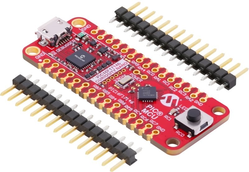
The PIC16F17146 Curiosity Nano Evaluation Kit is the best platform for rapid prototyping with the PIC16F17146 family of MCUs. This USB-powered kit features an on-board programmer/debugger that seamlessly integrates with MPLAB® X Integrated Development Environment (IDE). Its small form factor makes the board excellent for breadboard soldering, or you can combine it with the Curiosity Nano Base for Click boards™, which features multiple mikroBUS™ sockets so you can easily add sensors, actuators or communications interfaces from Mikroelektronika’s extensive selection of Click boards.

System Features
Configurable Analog
12-bit ADCC, Op Amp (OPA), 8/10-bit DAC, Zero Cross Detect (ZCD)
The intelligent Analog-to-Digital Converter with Computation (ADCC), configurable operational amplifiers (OPAs), high-speed analog comparators, multiple Digital-to-Analog Converter (DACs) and a Zero Cross Detect (ZCD) peripheral offer a high level of analog integration for amplification, filtering and signal conditioning for sensing and measurement applications. High-resolution ADC conversions with strong noise rejection and automated analog signal analysis and data acquisition functions for enhanced real-time system response are achieved with the 12-bit differential ADC with Computation. The programmable gain settings of the on-chip operational amplifiers reduce the cost and space required by external components in applications that require a gain stage before A-D conversions.
Layout Flexibility
Peripheral Pin Select (PPS)
Peripheral Pin Select (PPS) provides the ultimate flexibility when routing digital signals to device pins. With PPS, any digital peripheral can be connected to any I/O pin on the fly for a customized layout. This allows you to maintain layout compatibility with older PIC® MCUs, even as new features are implemented.
Hardware Customization
Custom Logic and Interconnections
Configurable peripherals can be easily customized to fit your application needs. The 8-bit virtual port interconnects digital peripherals without requiring any external pins to enable rapid responses to changing events in commonly used control systems. The Configurable Logic Cell (CLC) is a user-configurable peripheral for creating custom hardware-based logic functions. It allows you to integrate a combination of external and internal signals as inputs and connect on-board peripherals to reduce the number of external components needed for your design, which reduces your PCB footprint and overall system cost.
Safety First
Functional Safety Ready
The CRC/SCAN module and the Windowed Watchdog Timer (WWDT) work in tandem to provide the necessary tools to incorporate functional safety into your application. By ensuring the integrity of the program Flash contents, these devices support the implementation of safety standards such as Class B and UL 1998.
Improved System Response
Core Independent Peripherals (CIPs)
Configurable CIPs require almost no additional code and no additional components to enable this family of MCUs to handle and accomplish mission-critical and time-sensitive tasks smoothly entirely without CPU intervention. They save Flash memory and allow you to use the CPU’s resources to run complex systems as efficiently as possible. This combination of benefits simplifies your design while reducing power consumption and increasing system responsiveness.