Read While Write (RWW) Memory Explained in a Flash
Check out this post for an overview of RWW memory.

Harvard Architecture: Revolutionizing Computing Speeds
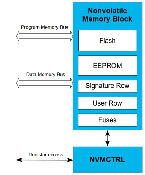
The Harvard architecture was a revolution in the computing world that split system memory into two separate banks: program memory and data memory. Normally, each bank gets its own memory bus, which enables unidirectional communication: each memory bank could be read or written to (but not read and written at the same time). The greatest advantage of this memory division was instead of a single bus needing to take turns between reading/writing data and fetching the next Central Processing Unit (CPU) instruction, the Harvard architecture allowed reads or writes to data memory while the CPU was running off instructions being simultaneously read from the program memory since the two banks were divided, resulting in greatly improved processing times.

Where RWW Comes In
The Harvard architecture worked great for speeding up processing times when data memory was constantly changing but fell short if the program memory needs to change, since it still bottlenecked by the unidirectional nature of the program memory bus. If the program memory data needs to be changed, the CPU halts since no instructions can be read while the program memory bus is busy writing to the program memory bank. As the name implies, RWW allows the program memory bus to be both read and written to at the same time, enabling the CPU to continue to run while its own memory is updated.
How RWW Works
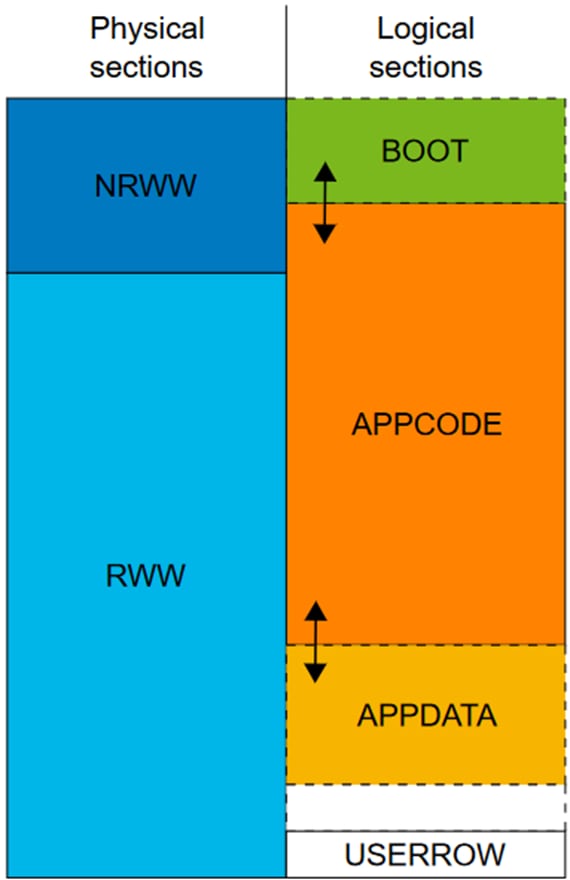
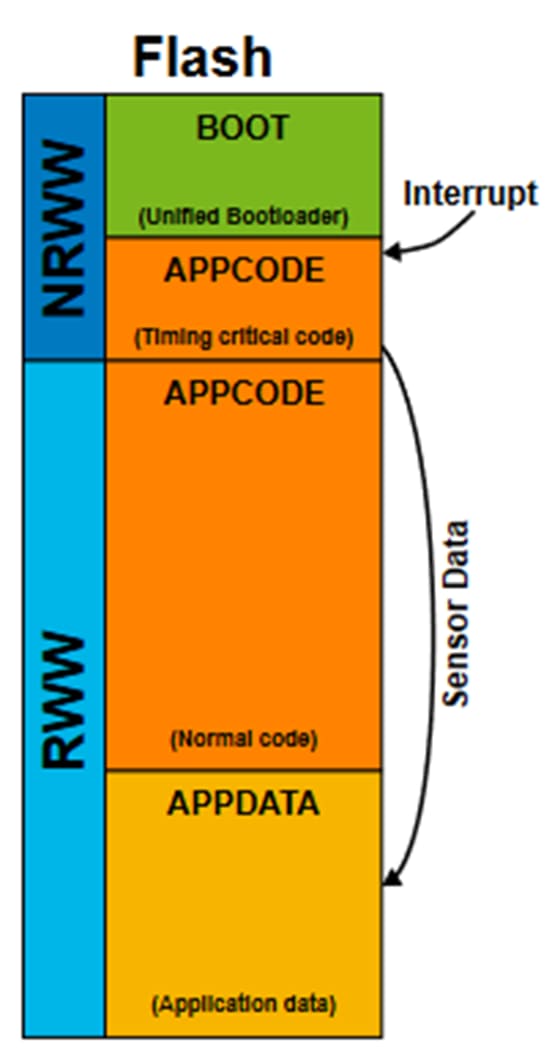
The new AVR® EA device comes with RWW, so we’ll cover its specific implementation of RWW. By dividing the program memory into two sections and expanding the program memory bus, data can be written to the RWW section, while the CPU operates off the instructions simultaneously read from the Non-RWW (NRWW) section.

This capability allows the program code to be updated on-the-fly without pausing the program, which is great for OTA updates, fast bootloader operation and even data logging in your program memory section to maximize your flash usage instead of needing an external EEPROM. Knowing what your application needs will help you determine the best way to use your RWW functionality.
The table below shows the conditions in which a flash section can be read while another section is being erased and written to. By running code in the NRWW section, the RWW section can be updated without halting the CPU by tying up the memory bus.

With such a change in architecture comes technical hurdles, such as handling interrupts. If you program your microcontroller and your interrupt exists in a part of memory that is RWW, what happens if they get overwritten during operation? The solution is to move your interrupts and interrupt callbacks to NRWW memory where they are in a known location to preserve their integrity. TB3344, by Henrik Arnesen and Egil Rotevatn, covers how to do this in-depth. It dives into best coding practices, important memory address and shows timing diagrams of RWW in action when servicing interrupts.

If you see the additional speed, flexibility and functionality that comes with RWW helping you in your next design, be sure to check out our latest AVR® EA line of microcontrollers.