Motor Current Sensing With the LX4580 Motor Controller and Data Acquisition System
Learn more about the LX4580 analog front-end Integrated Circuit (IC) for actuation systems and the requirements and tradeoffs for ground-side current sense amplifiers.

The LX4580 is an analog front-end for high-reliability motor-actuator control systems working under stringent standards such as DO-160 for avionics in airborne systems. The LX4580 interfaces with dual microcontrollers (MCUs) or Field-Programmable Gate Arrays (FPGAs) in redundant COM/MON system architectures and features Error Correcting Code (ECC) encoding to provide 1-bit error correction and 2-bit error detection. Sequential logic is implemented with Triple-Mode Redundancy (TMR) to protect against Single-Event Upsets (SEUs).
The block diagram below shows a typical motor-actuator system using a resolver to provide accurate Permanent Magnet Synchronous Motor (PMSM) rotor position, and a Linear Variable Differential Transformer (LVDT) for actuator linear position feedback. The LX4580 combines analog sensor acquisition and motor control Pulse-Width Modulation (PWM) synthesis. For the motor control, there are eight independent PWM outputs to drive upper and lower FET gate drivers in the motor half-bridge stages. FET drivers and current sense amplifiers are usually the only external active components required.

This is the second post in a series discussing various topics around LX4580 implementations. The previous post discusses needs and tradeoffs when selecting the FET drivers, and this follow-up piece will cover the same for the ground-side current sense amplifiers shown in the block diagram above.
The LX4580 includes five current sense interfaces via five dedicated Σ-Δ Analog-to-Digital Converters (ADCs). That's enough current sensing for each half-bridge driving a two-phase bipolar stepper motor or up to four-phase brushless DC motor, plus an extra current sense for high-side monitoring the total motor supply current at the motor supply rail. The analog front-ends are identical for the five current sense inputs and comprise a differential input with a ±1.1V full scale with respect to a common reference input, ISENSE_RTN, as shown below.

The differential inputs simplify the use of common galvanically isolated current sensing techniques, such as current transformers, Rogowski coils and Hall-effect sensors, all commonly used to meet safety regulations by electrically separating high voltage from low voltage systems.
Here we'll look at probably the lowest cost current sensing technique, that of using current sense resistor in the ground side of a half-bridge, as shown in the block diagram above. Current sense resistors are chosen to drop the smallest reasonable voltage, in the order of 10s to 100s of mV, to minimize wasted power. Amplification is therefore commonly needed to make the full scale current sense voltage match the ADCs input range (±1.1V for LX4580). There are two standard approaches to providing this gain with an operational amplifier (op amp): a single-ended non-inverting amplifier, and a differential amplifier. Here's the non-inverting amplifier approach, amplifying the sense voltage, VP, with respect to PGND by Gain = 1 + R2⁄R1:

At a glance, it would appear that the non-inverting amplifier approach will work fine, taking care to use Kelvin (4-terminal) sensing to Rsense on the PCB layout for accuracy. Unfortunately, there's also a measurement error incurred by PGND (the sense resistor GND) and AGND (the amplifier and ADC input's GND) not being at the same potential, due to realities of layout. Just 100µV of (noisy) difference between AGND and PGND for a 100mV sense voltage corresponds to 1 bit in a 10 bit measurement system.
The differential amplifier approach solves the ground problem by level shifting the measurement from PGND at the inputs to AGND at the output. The amplifier amplifies the actual sense voltage VP - VN by Gain = 1 + R2⁄R1, rather than presuming that VN is at AGND potential.

The classic use case for a differential amplifier is to extract a small signal riding on top of a large signal, itself often modulating. An important amplifier figure of merit here is common-mode rejection ratio, or CMRR, which is the amount of this unwanted common signal that passes through the amplifier. In the case of grounded current sensing, however, the common-mode voltage varies from 0V (when no current is passing through the current sense resistor), to half the maximum voltage drop at full current. This is a much smaller common-mode voltage than usually the case for the classic use case, which might have a ±10mV signal riding on a ±10V carrier.
Poor matching between the inverting and non-inverting gains, caused by resistor tolerances, causes poor CMRR in a differential amplifier. If all four resistors have a tolerance t, then the worst-case gain mismatch is 4t. This occurs when the R2⁄R1 ratio for the non-inverting network is at toleranced maximum or minimum, and the R2⁄R1 ratio for the inverting network is at the opposite toleranced extreme.
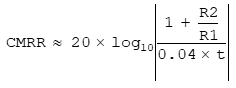
where t is resistor tolerance in % (ref: Sergio Franco)
Note that increasing the closed loop gain (the R2⁄R1 term above) increases CMRR.
To create an example, let's consider a case where we plan a 100mV drop across the current sense resistor. We need an amplifier gain of 11 to meet the LX4580's ±1.1V ADC input range. This means that we need to choose the ratio R2⁄R1 = 11 for the differential amplifier.
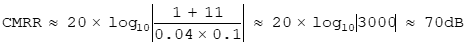
Since the common mode voltage is half the input voltage, so 50mV at 100mV full scale, the effective input error due to limited common mode rejection is 50mV⁄3000 = 16.6µV at full scale.
Now looking at amplifier choices, a typical list of requirements is:
- Operation from a single low voltage supply already used in the system, such as 5V
- Low enough input offset voltage and input offset drift with temperature
- Sufficient gain-bandwidth and output slew rate to follow the current changes
- Low CMRR
- A high-reliability build standard, such as AEC-Q100
One example is the AEC-Q100 qualified MCP6V91 op amp family. The supply range is 2.24V to 5.5V, making it suitable to operate from the LX4580's 5.25V supply for auxiliary circuits. Input offset is better than ±12µV max over the -40°C to +125°C temperature range. Typical gain-bandwidth is 10MHz.
Here's an example 3-phase current sense implementation using MCP6V91 amplifiers. Duals (MCP6V92) or a quad (MCP6V94) could be used instead, as layout permits.

The input resistors to the three x11 gain stages are split to allow capacitors to be used for simple common mode noise filtering. The corner frequency is a tradeoff between filter effectiveness and latency in current measurement. The amplifier themselves will have a typical corner frequency of 10MHz⁄11 = 910kHz.
f3db = 1⁄2 × π × (2 × 1.5KΩ × 470pF) = 113kHz
The ISENSE_RTN pin has a working input range of 1.2V to 3.8V. The MCP6V91 amplifier has a common mode input voltage range ranging from below ground to its supply - 1.3V, so a little less than 4V with a 5.25V supply. The MCP6V91 amplifier output is rail-to-rail. Biassing ISENSE_RTN and the differential amplifiers to 1.25V set the amplifier outputs at 1.25V ±1.1V full scales for positive and negative currents, matching the Σ-Δ ADC input range.
Now looking at error budgets, with respect to the 100mV positive full scale input, we have input errors due to:
- CMRR error of 16.6µV with choice of 0.1% resistors
- Amplifier input offset error of 12µV
- Amplifier CMRR error of 68dB minimum, so 50mV⁄2512 = 19.9µV
So total input-referred amplifier error is 48.5µV, or 1 part in 2062 with respect to 100mV full scale, which is a ±1 bit error in a 12 bit acquisition system. The worst case gain error due to resistor mismatch is ±0.4%, which is a ±1 bit error in a 8 bit acquisition system. The gain error can be improved be using higher tolerance (or matched) resistors, or using a calibration procedure to measure the actual gains and compensate with scaling factors in firmware.
For more information, please visit our LX4580 web page.