Loading
Log in to myMicrochip to access tools and benefits. Sign up in just one minute.
Maximize Your Experience: Reap the Personalized Advantages by Completing Your Profile to Its Fullest. Update Here
Stay in the loop with the latest from Microchip. Update your profile while you are at it. Update Here
Complete your profile to access more resources. Update Here
Designed for Demanding Analog Applications
The AVR® DB series builds upon the low-power performance of the AVR core with a world-class selection of Core Independent Peripherals (CIPs) and a fully loaded Intelligent Analog portfolio, giving you the freedom to design tomorrow’s solutions today. Featuring three on-chip operational amplifiers (op amps), this family is unparalleled in its signal conditioning capabilities. With its Multi-Voltage I/O (MVIO), the AVR DB is a perfect companion microcontroller (MCU) in complex designs with multiple power domains.
This family of MCUs leverages on-board CIPs and a 5V operation mode for increased noise immunity while also reducing system latency by making use of the powerful Event System and Configurable Custom Logic (CCL) peripherals. The AVR DB family’s MVIO allows true level-shifted bi-directional communication with devices on a different power domain. You can use the AVR DB family for real-time control functions in industrial control, home appliance, automotive, Internet of Things (IoT) and other applications. For low-latency control applications and capacitive touch user interfaces, our AVR DA MCUs are a great option.
Getting Started
The AVR128DB48 Curiosity Nano Evaluation Kit is the best platform for rapid prototyping with AVR DB MCUs. This USB-powered kit features an on-board programmer/debugger that seamlessly integrates with the MPLAB® X Integrated Development Environments (IDEs). Its small form factor makes the board excellent for breadboard soldering, or you can combine it with the Curiosity Nano Base for Click boards™, which features multiple mikroBUS™ sockets so you can easily add sensors, actuators or communications interfaces from Mikroelektronika’s extensive selection of Click boards.
*This board is based on the 128 KB 48-pin AVR DB MCU. An evaluation kit with the 64-pin AVR DB is not available.
Functional Safety Ready for Safety-Critical Applications
The AVR DB family is recommended for safety-critical applications targeting both industrial and automotive products (IEC 61508 and ISO 26262). We also offer the MPLAB XC8 Functional Safety Compiler License, which is a TÜV SÜD certified compiler package that supports 8-bit PIC® and AVR microcontrollers. Documents such as FMEDA reports and safety manuals are available on request. Please contact your local Microchip sales office or your distributor for more information.

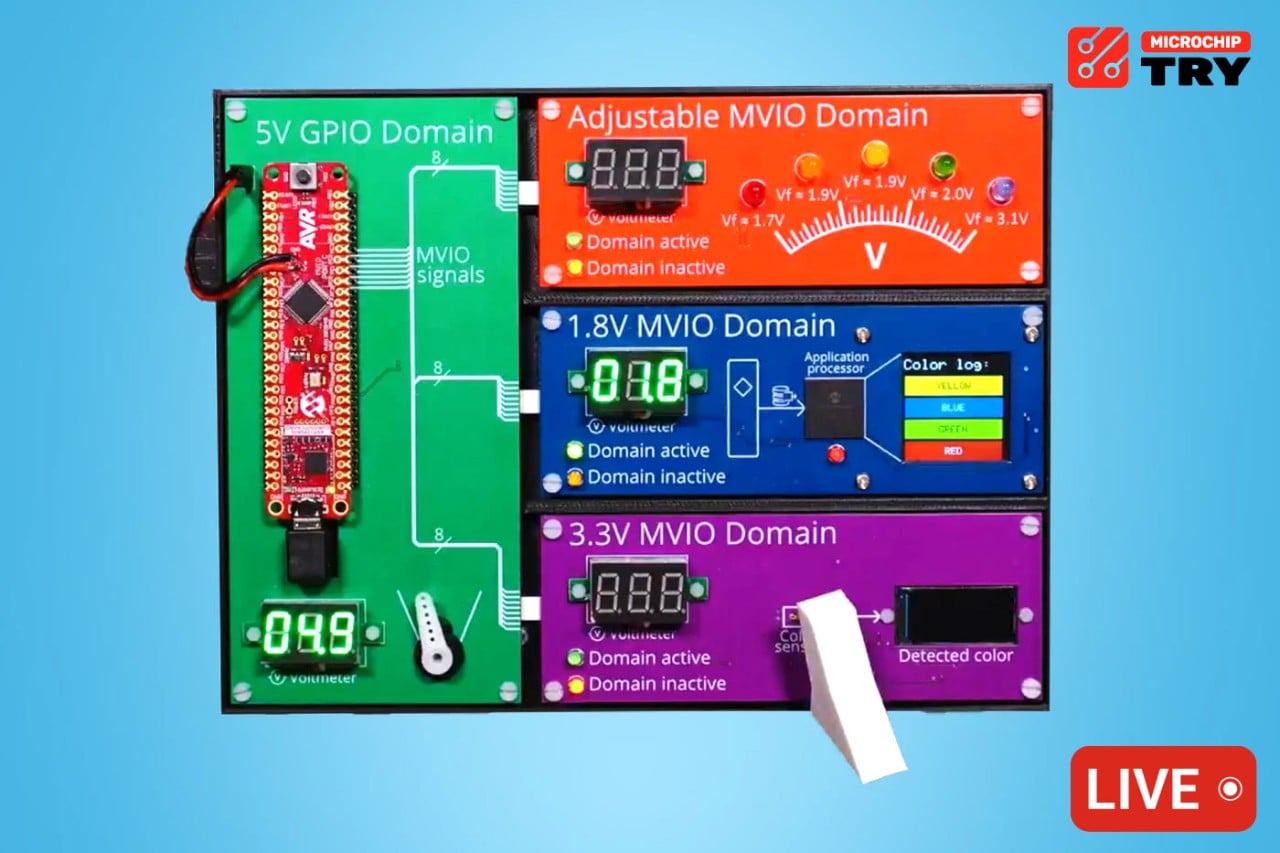
Try a Live AVR DB Demo
Microchip Try is a website for visual learners that provides real-time demos that you can interact with by changing variables and watching how the demo responds.
Explore the MVIO demo and the Op Amp Overcurrent Detection demo, engage with them and learn how to implement these features in your design.
System Features
On-Chip Level Shifters
Multi Voltage I/O (MVIO)
The Multi Voltage I/O (MVIO) system powers Port C and allows it to operate at a different voltage than the rest of the device. This greatly simplifies communication with other devices that might be running at a different voltage without the need of expensive external level shifters. If voltage is dropped on the VDDIO2 pin, an interrupt can be issued notifying the main application that the MVIO system is currently unpowered and not able to operate. If you do not want to use MVIO, VDDIO2 should be connected to VDD.
Analog Signal Conditioning
Operational Amplifier (OPAMP)
The Analog Signal Conditioning (OPAMP) peripheral features three operational amplifiers (op amps). These op amps are implemented with a flexible connection scheme using analog multiplexers and resistor ladders. This allows a large number of analog signal conditioning configurations to be achieved, many of which require no external components
Integrated Analog
12-bit ADC, 10-bit DAC, ZCD, Analog Comparator
The on-board 12-bit, 130 ksps differential Analog-to-Digital Converter (ADC) features selectable internal voltage references with minimal temperature drift. Using the Event System, the on-board Analog Comparator (AC) can be connected to trigger autonomous operation in other peripherals, which is ideal for real-time control and closed-loop operations. The output of the 10-bit Digital-to-Analog Converter (DAC) can either be sent to a pin or it can be used to generate an adjustable reference voltage for the AC
Robust Crystal Oscillator
Clock Failure Detect (CFD)
The Clock Failure Detect (CFD) is a system supervisory circuit that will switch over to the internal clock if the external crystal fails (stops). This additional safety level allows the device to run on a very precise clock. If the crystal fails, the device automatically switches to a secondary internal clock source and generates an interrupt to notify the main application that the external crystal has stopped. The user can then determine if the application needs to stop or go into a safe mode.
Hardware Customization
Custom Logic
The Custom Logic peripheral is a programmable logic peripheral that can be connected to the device pins, events or other internal peripherals. Each Lookup Table (LUT) consists of three inputs: a truth table, an optional synchronizer and a filter and edge detector. An LUT can generate an output to be routed internally or to an I/O pin, which eliminates the need for external logic and reduces BOM cost.
Real Time Response
Event System
The Event System allows peripherals to communicate directly with each other without involving the CPU or bus resources. This means that different triggers at the peripheral level can result in an event, such as a timer’s interrupts triggering an action in another peripheral. The Event System has three independent channels for direct peripheral-to-peripheral signaling. This deterministic signaling method is a perfect fit for real-time applications. The events are handled at the peripheral level even if the CPU is occupied handling interrupts or in sleep mode.
Safety First
CRC, WWDT, FMEDA, BOD, POR, VLM
You can use the built-in features that support safety-critical applications to add robustness and reliability to your design. These include the Windowed Watchdog Timer (WWDT) for system supervision, the Cyclic Redundancy Check (CRC) for scanning Flash memory, and the Event System for fault detection. Other features include a Voltage Level Monitor (VLM), a Brown-Out Detector (BOD) and Power-On Reset (POR) for monitoring the supply voltage.